AI technical title is built by Patsnap AI team. It summarizes the technical point description of the patent document.
a manufacturing method and semiconductor technology, applied in the direction of semiconductor devices, electrical equipment, basic electric elements, etc., can solve the problem of high manufacturing cost of the substrate itself, and achieve the effect of high bonding strength
Active Publication Date: 2016-07-14
SICOXS +1
View PDF25 Cites 14 Cited by
Summary
Abstract
Description
Claims
Application Information
AI Technical Summary
This helps you quickly interpret patents by identifying the three key elements:
Problems solved by technology
Method used
Benefits of technology
Benefits of technology
The invention provides a way to make semiconductor wafers that are strongly bonded together without creating a layer of oxide at the bonded interface. This technique can also work on wafers that have difficulty in being smoothed.
Problems solved by technology
However, the manufacturing cost of the substrate itself is expensive, which has been an obstacle to practical application.
Method used
Image
Click on the blue label to locate the original text in one second.
Reading with bidirectional positioning of images and text.
Examples
embodiment
Configuration of Bonded Substrate
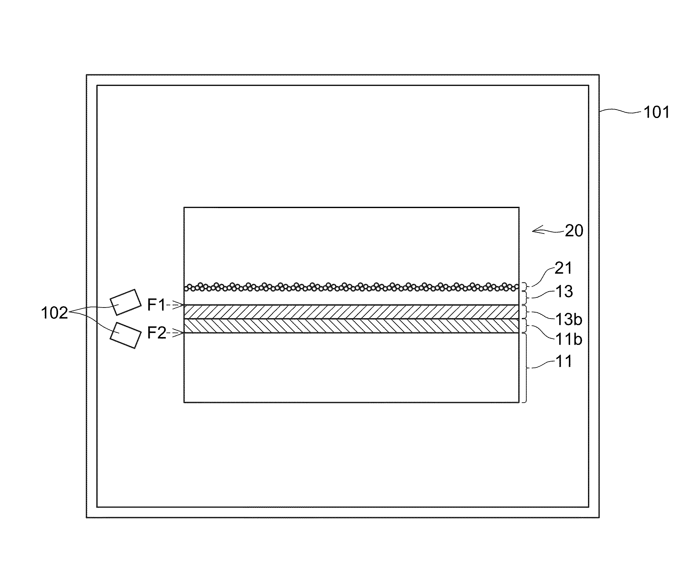
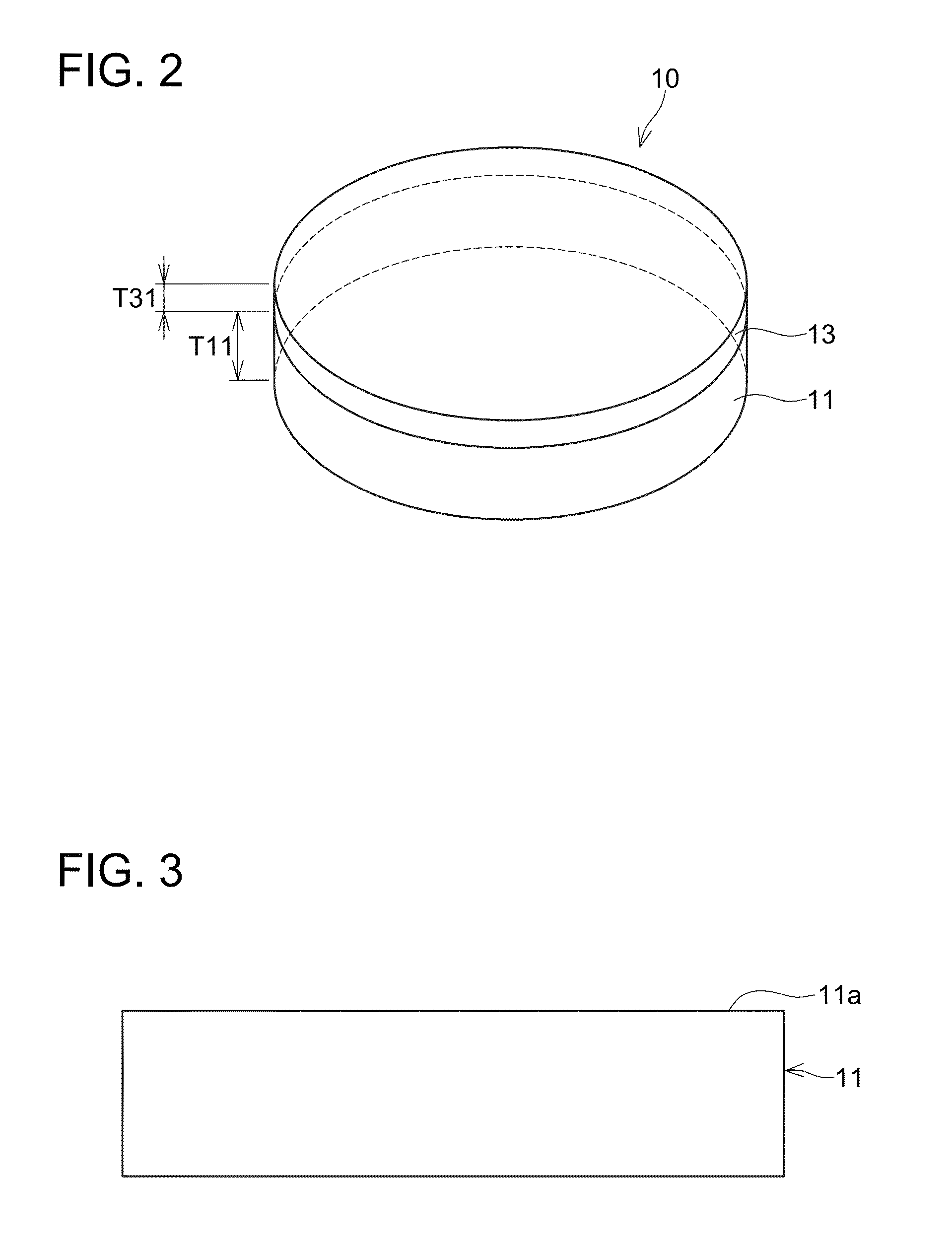
[0026]FIG. 2 is a perspective view of a bonded substrate 10 according to the present embodiment. The bonded substrate 10 has an approximately disc-like shape. The bonded substrate 10 includes a support substrate 11 disposed on the underside, and a semiconductor layer 13 bonded to the upper surface of the support substrate 11. The semiconductor layer 13 may be formed from, for example, single crystals of a compound semiconductor (e.g., 6H-SiC, 4H-SiC, GaN, AlN). Alternatively, it may be formed from single crystals of a mono-element semiconductor (e.g., Si, C).
[0027]For the support substrate 11, various materials can be used. It is preferable that the support substrate 11 is resistant to various thermal processes applied to the semiconductor layer 13. Additionally, it is preferable that the support substrate 11 is formed from a material with a small difference in thermal expansion coefficient between the semiconductor layer 13 and this substrate 11. Fo...
modified example
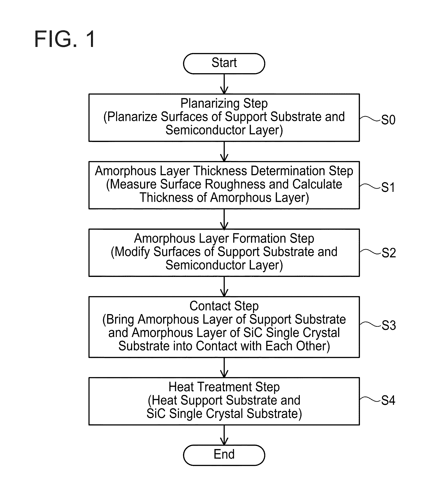
[0057]In the amorphous layer formation process (step S2), the method for forming an amorphous layer is not limited to irradiating an argon neutral atom beam. For example, a method for injecting atoms, molecules, ions, or the like such as He, H, Ar, and C may be employed.
[0058]In the heat treatment process (step S4), an aspect of a temperature change with a processing time may be varied.
[0059]The material used in the support substrate 11 is not limited to polycrystalline SiC. Any material that withstands various heat processes applied to the semiconductor layer 13 suffices. For example, a sintered body formed of a mixture of ceramic materials also suffices. The ceramic materials to be used may be varied. At least one material selected from, for example, SiC, Si, AlN, Al2O3, GaN, Si3N4, SiO2, Ta2O5 and so on, may be used.
PUM
Abstract
A technique disclosed herein relates to a manufacturing method for a semiconductor substrate having the bonded interface with high bonding strength without forming an oxide layer at the bonded interface also for the substrate having surface that is hardly planarized. The manufacturing method for the semiconductor substrate may include an amorphous layer formation process in which a first amorphous layer is formed by modifying a surface of a support substrate and a second amorphous layer is formed by modifying a surface of a single-crystalline layer of a semiconductor. The manufacturing method may include a contact process in which the first amorphous layer and the second amorphous layer are contacted with each other. The manufacturing method may include a heat treatment process in which the support substrate and single-crystalline layer are heat-treated with the first amorphous layer and the second amorphous layer being in contact with each other.
Description
TECHNICAL FIELD[0001]This application claims the priority of Japanese Patent Applications No. 2013-142151 filed on 5 Jul. 2013. The content thereof is incorporated herein by reference in its entirety. This specification discloses a technique relating to a manufacturing method for a semiconductor substrate having a bonded interface with high bonding strength.BACKGROUND ART[0002]As a candidate for the substrate material of the next power device, siliconcarbide (hereinafter referred to as SiC) is suggested. However, the manufacturing cost of the substrate itself is expensive, which has been an obstacle to practical application. Meanwhile, if only a device formation layer part uses high quality single-crystalline SiC, and this part can be fixed to a support substrate (a material which is strong, heat-resistant, and clean, e.g., Poly-SiC, which withstands device manufacturing processes) in some way, it is possible to form a base material meeting both low cost (support substrate part) an...
Claims
Application Information
Patent Timeline
Application Date:The date an application was filed.
Publication Date:The date a patent or application was officially published.
First Publication Date:The earliest publication date of a patent with the same application number.
Issue Date:Publication date of the patent grant document.
PCT Entry Date:The Entry date of PCT National Phase.
Estimated Expiry Date:The statutory expiry date of a patent right according to the Patent Law, and it is the longest term of protection that the patent right can achieve without the termination of the patent right due to other reasons(Term extension factor has been taken into account ).
Invalid Date:Actual expiry date is based on effective date or publication date of legal transaction data of invalid patent.

