Manufacturing method of ultra-thin semiconductor device package assembly

a manufacturing method and semiconductor technology, applied in semiconductor devices, semiconductor/solid-state device details, electrical devices, etc., can solve the problems of short current path, less resistance, and more easily warpage of wafers, so as to facilitate the disclosure of instant disclosure

Active Publication Date: 2016-07-21
NIKO SEMICON +1
View PDF8 Cites 2 Cited by
  • Summary
  • Abstract
  • Description
  • Claims
  • Application Information

AI Technical Summary

Benefits of technology

[0005]The object of the instant disclosure is to provide a manufacturing method of an ultra-thin semiconductor device package structure. The method comprises the following steps. Firstly, a wafer having a plurality of semiconductor devices is provided. One of the semiconductor devices, a first semiconductor device, has an active surface and a back surface. The active surface includes an active region and an outer region. A first electrode and a second electrode are arranged in the active region, and the outer region is divided into a cutting portion and a channel portion. Subsequently, a patterned protecting layer having a plurality of openings is formed on the active surface to respectively expose the first electrode, the second electrode, and the outer region. Next, a trench is formed in the channel portion, in which the trench has a first depth less than a thickness of the wafer. Thereafter, a conductive structure is formed in the trench. In addition, a supporting board is provided, and the wafer is disposed on the supporting board with the active surface facing to the supporting board. Subsequently, a thinning process is performed upon the first semiconductor device from the back surface to expose the conductive structure, and then a back electrode layer is formed on the back surface of the first semiconductor device. The supporting board is separated from the wafer, and a plurality of contacting pads is formed on the active surface to respectively electrically connect the first electrode, the second electrodes and the conductive structure. Subsequently, a cutting process is performed on the cutting portion.
[0006]In order to further the understanding regarding the instant disclosure, the following embodiments are provided along with illustrations to facilitate the disclosure of the instant disclosure.

Problems solved by technology

In addition, thinning the base of the chip also can result in shorter current path and lower resistance so as to achieve higher power efficiency.
However, the thinner the wafer, the more easily the warpage of the wafer occurs.
The warpage may easily result in cracks in the wafer during the transportation or the fabricating process.

Method used


Image

  • Manufacturing method of ultra-thin semiconductor device package assembly
  • Manufacturing method of ultra-thin semiconductor device package assembly
  • Manufacturing method of ultra-thin semiconductor device package assembly

Examples


Embodiment Construction

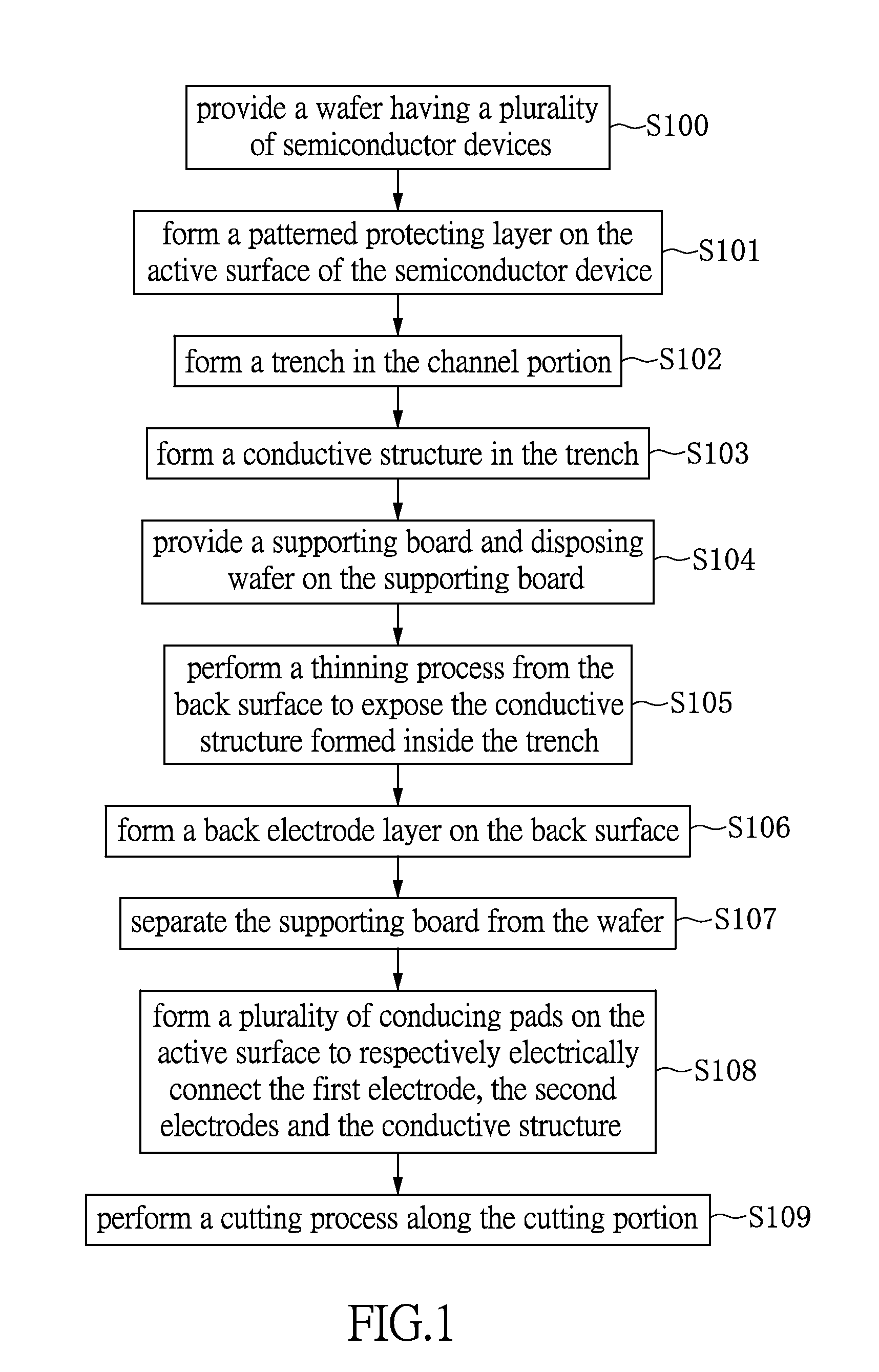
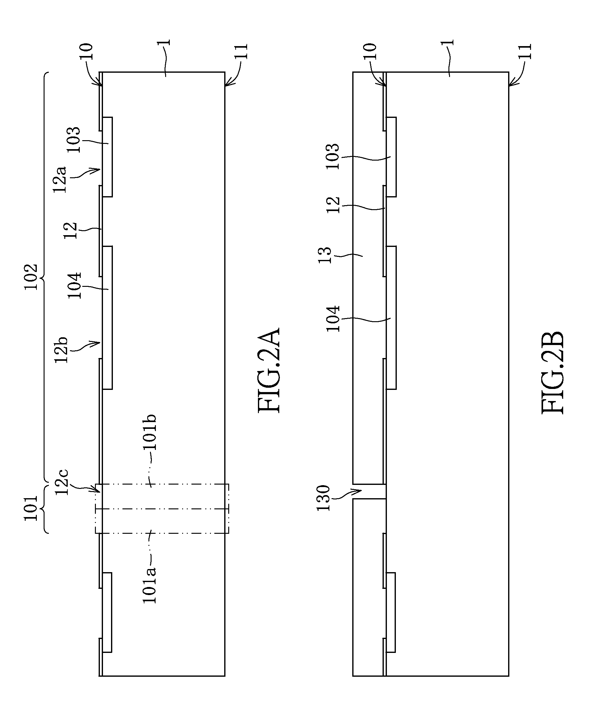
[0024]Please refer to FIG. 1. FIG. 1 shows a flow chart of the manufacturing method of an ultra-thin semiconductor device package structure in accordance with an embodiment of the instant disclosure. Please refer to FIGS. 2A to 2M, which respectively show sectional views of the ultra-thin semiconductor device package structure in different steps of the manufacturing method in FIG. 1 in accordance with one embodiment of the instant disclosure.

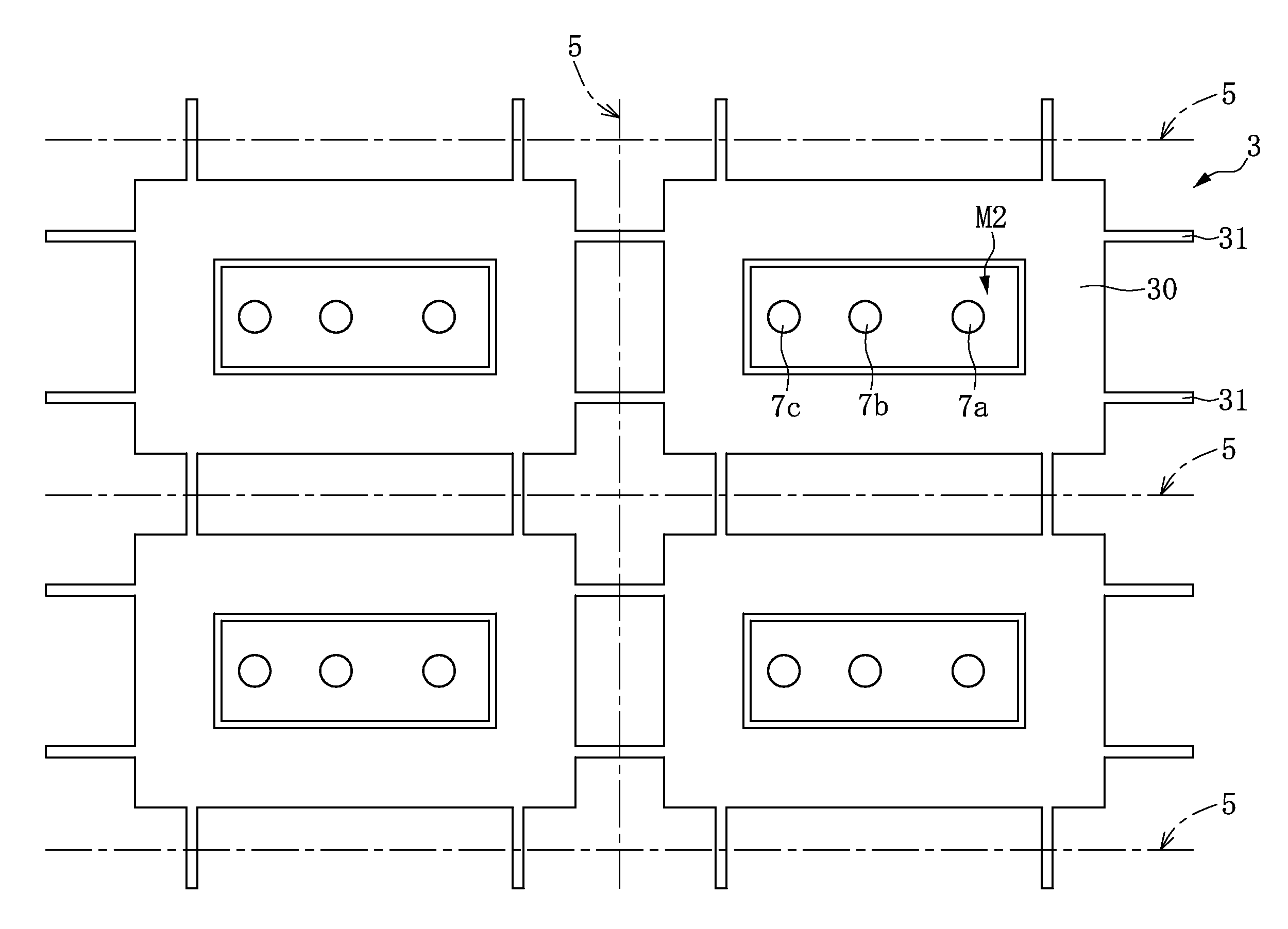
[0025]In step S100, a wafer having a plurality of semiconductor devices is provided. The wafer is usually made of Si or other semiconductor materials, such as GaAs. In the embodiment of the instant disclosure, the wafer 100 has a thickness of 250 to 700 μm. In the embodiment of the instant disclosure, the processes of fabricating the devices on the wafer 100 have been completed, and the wafer 100 includes a plurality of semiconductor devices.

[0026]In an embodiment, a package structure, which is fabricated by the manufacturing method of an ultra-...


PUM


Abstract

A manufacturing method of ultra-thin semiconductor device package structure is provided. Firstly, a wafer including a plurality of semiconductor devices is provided, and one of the semiconductor devices has an active surface having an active region and an outer region and a back surface. A first electrode and a second electrode are arranged in the active region, and the outer region has a cutting portion and a channel portion. Subsequently, a trench is formed in the channel portion, and filled with a conductive structure. The wafer is fixed on a supporting board, and then a thinning process and a deposition process of a back electrode layer are performed on the back surface in sequence. Thereafter, the supporting board is removed and a plurality of contacting pads is formed. A cutting process is performed along the cutting portion.

Description

BACKGROUND OF THE INVENTION[0001]1. Field of the Invention[0002]The instant disclosure relates to a semiconductor package process, in particular, to a manufacturing method of ultra-thin semiconductor device package assembly.[0003]2. Description of Related Art[0004]As the demand for power efficiency has become increasingly severe, chip structure design must be modified to improve the power efficiency. In addition, thinning the base of the chip also can result in shorter current path and lower resistance so as to achieve higher power efficiency. Under the conditions that the mechanical structure and the breakdown voltage of the vertical power device are not affected, thinning the wafer is an effective solution for reducing the resistance of the vertical power devices. However, the thinner the wafer, the more easily the warpage of the wafer occurs. The warpage may easily result in cracks in the wafer during the transportation or the fabricating process.SUMMARY OF THE INVENTION[0005]The...

Claims


Application Information

Patent Timeline
Patent Type & Authority Applications(United States)
IPC IPC(8): H01L23/00H01L23/495H01L21/78H01L29/66H01L21/683H01L21/768
CPCH01L24/97H01L21/6835H01L21/76802H01L21/76877H01L21/78H01L29/66666H01L2224/32245H01L24/83H01L23/49562H01L2221/68359H01L2221/6834H01L2221/68381H01L2224/838H01L21/76843H01L2221/68327H01L23/495H01L21/76898H01L2224/92242H01L24/03H01L24/05H01L24/06H01L24/11H01L24/29H01L24/32H01L24/73H01L24/94H01L2224/02372H01L2224/0345H01L2224/03452H01L2224/03462H01L2224/0347H01L2224/0391H01L2224/0401H01L2224/04026H01L2224/05582H01L2224/05639H01L2224/05647H01L2224/05655H01L2224/06181H01L2224/1132H01L2224/11462H01L2224/16227H01L2224/29111H01L2224/83192H01L2224/83862H01L2224/94H01L2224/97H01L2224/05568H01L2224/05583H01L2224/05548H01L2224/05155H01L2224/05166H01L2224/05567H01L2224/13022H01L2224/13024H01L2224/2929H01L2224/73253H01L29/7827H01L24/02H01L2224/02311H01L2224/02313H01L2224/05082H01L2224/05073H01L2224/0239H01L2224/036H01L2224/03914H01L2224/03002H01L2224/29294H01L2224/293H01L24/92H01L2224/133H01L2224/13294H01L2224/29299H01L2224/81191H01L2224/8321H01L24/13H01L2224/05184H01L2224/05147H01L2224/131H01L2224/03H01L2924/00014H01L2924/013H01L2224/83H01L2224/81H01L2924/01022H01L2924/01074H01L2924/01029H01L2224/0231H01L2224/27H01L2224/11H01L2924/014
Inventor HSIEH, CHIH-CHENGHSU, HSIU-WEN
Owner NIKO SEMICON
Why Eureka
Try Eureka