Transparent computer structure

Inactive Publication Date: 2016-07-28
SIGNIFY HOLDING B V
View PDF3 Cites 0 Cited by
  • Summary
  • Abstract
  • Description
  • Claims
  • Application Information

AI Technical Summary

Benefits of technology

The present invention aims to enhance the flexibility of communication between components in an electronic device. The technical effect of the invention is to provide greater efficiency and flexibility in data transfer and communication within the device.

Problems solved by technology

With increasing complexity of both integrated circuits as well as of circuits comprising discrete components arranged on a PCB follows problems related to the communication between components.
The addition of metal layers in integrated circuits leads both to a more complex manufacturing process and to problems associated with heat dissipation from components.
Similarly, with an increasing number of discrete components on a PCB, the connection paths becomes more complex while the area of the PCB may be limited, which may in turn lead to limitations in functionality of the circuit.
However, as the size of the electrical connections is reduced the resistance increases which in turn leads to more heat generation and thereby to power losses in the circuit.
To keep up with the higher demands, the number of components in electronic devices therefore increases, which means the number of possible and required connections and contacts in the device grows rapidly and thus also the overall complexity of the circuit.

Method used


Image

  • Transparent computer structure
  • Transparent computer structure
  • Transparent computer structure

Examples


Embodiment Construction

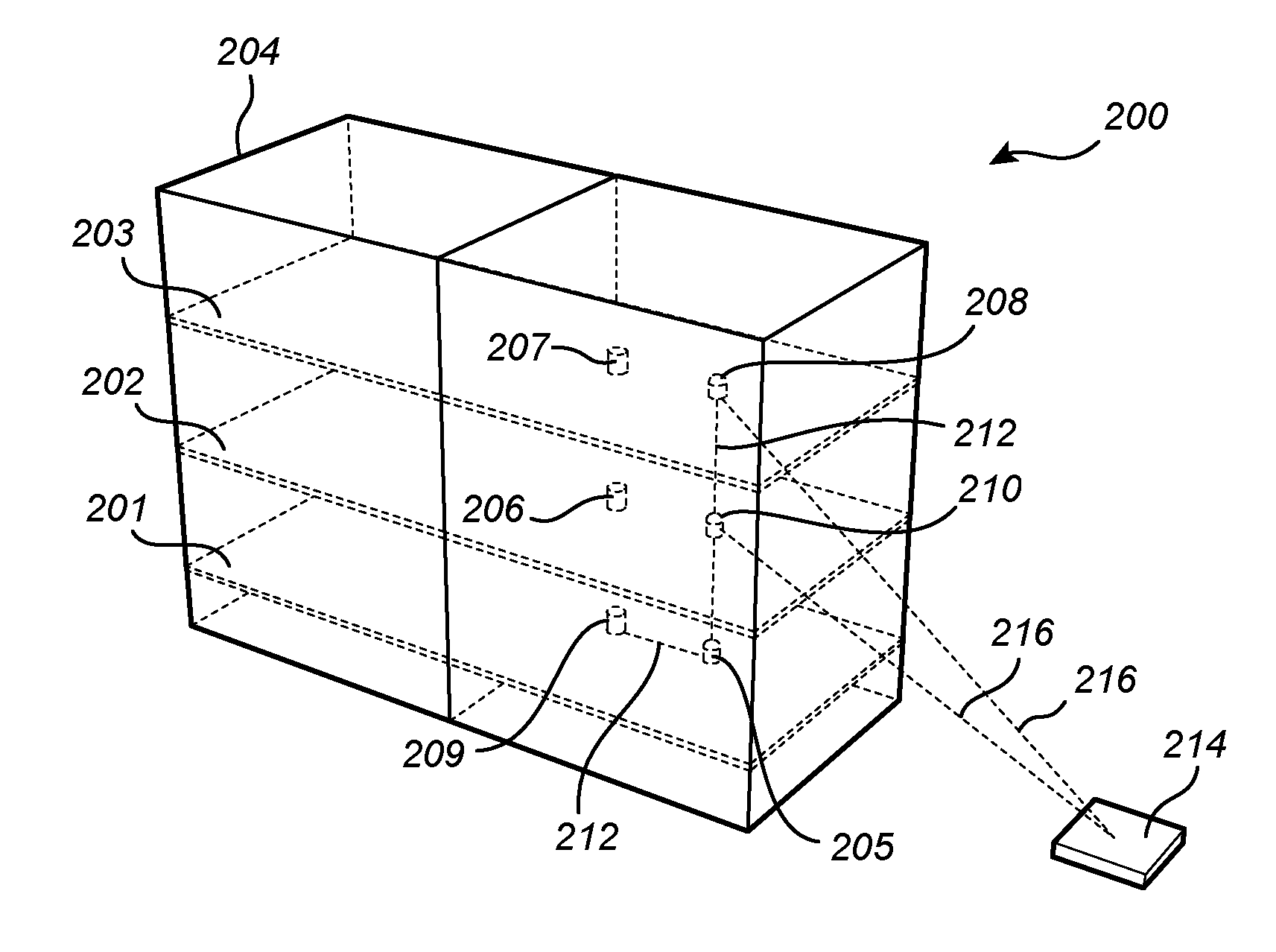
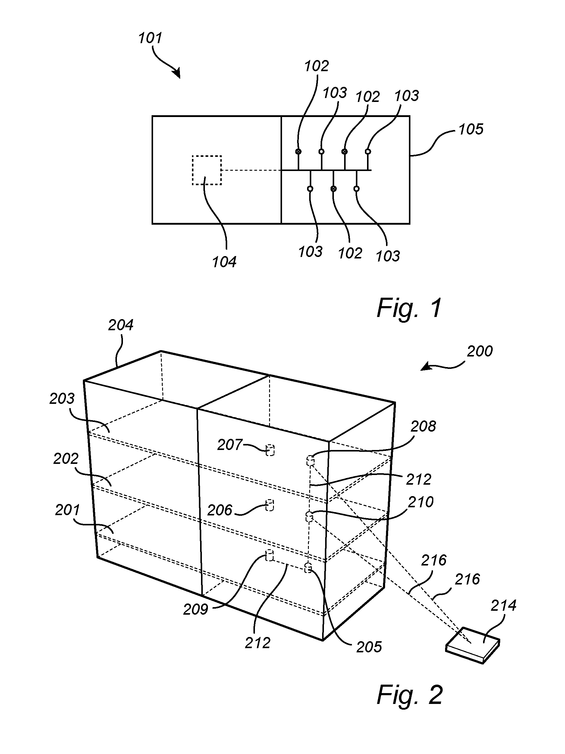
[0026]In the following description, the present invention is described with reference to example applications. It should, however, be noted that this by no means limits the scope of the invention, which is equally applicable to other applications, such as light equipments, LED lamps, coded light luminaires, mobile phones, watches, heads-up displays, television sets, displays, and games.

[0027]FIG. 1 illustrates an exemplary embodiment of an electronic device 101 in accordance with the invention in the form of a computer bus 101. FIG. 1 shows a circuit board 105, a processing unit 104, a plurality of light-emitting devices 102, and a plurality of optically transmissive light-receiving device 103. The light-receiving devices 103 are optically transmissive and are arranged on the circuit board 105 which also is optically transmissive. The light emitting devices 102 are also arranged on the circuit board 105. The light-emitting devices 102 communicate with the light-receiving devices 103...


PUM


Abstract

An electronic device (101, 200, 300, 400) is provided comprising optically transmissive electrical components (102, 103, 205-210, 303, 304, 405-410, 413-418) and optically trans missive computer structures such as boards (105, 201-203) or enclosures (302, 311-313). The components of the electronic device communicate through optical signals (212, 214, 309, 314, 422, 428) that propagate freely within the electronic device. That is, the optical signals are not guided and may or may not travel through the optically transmissive structures and components. This enables increased communication paths and reduced number of physical connections between various parts of the electronic device. The components may be placed in a single plane or in a three-dimensional layout and still communicate via the light signals. The invention enables an adaptable layout of an electronic device which is easily constructed.

Description

FIELD OF THE INVENTION[0001]The present invention relates to electronic devices. In particular, the present invention relates to communication in electronic devices.BACKGROUND OF THE INVENTION[0002]In modern electronic devices, a large number of electronic components are electrically connected for communicating with each other. In some applications, discrete components are mounted on a printed circuit board (PCB) which comprises the required conductive paths for interconnecting the components. For more complex applications where a larger number of components are required, integrated circuits are used where components are made in a semiconductor substrate and where communication between components takes place in different metal layers arranged on the substrate.[0003]With increasing complexity of both integrated circuits as well as of circuits comprising discrete components arranged on a PCB follows problems related to the communication between components. In an integrated circuit com...

Claims


Application Information

Patent Timeline
IPC IPC(8): H04B10/80G01J1/04H05K1/14H01L31/032H01L25/16H05K1/02G01J1/02H01L31/113
CPCH04B10/801G01J1/0271G01J1/0407H01L31/1136H01L31/032H05K2201/10121H05K1/0274H01L25/165H05K1/14H05K2201/10106H05K2201/10151H01L25/167G02B6/43H01L2924/0002H01L2924/00
Inventor GUILLANNEUF, FREDERIC ALEXANDREKRIJN, MARCELLINUS PETRUS CAROLUS MICHAEL
Owner SIGNIFY HOLDING B V
Why Eureka
Try Eureka