Optical modulating device having gate structure

a technology of optical modulators and gate structures, applied in the field of optical modulators, can solve the problems of slow operation response times of such optical modulators and may reach more than several s

Active Publication Date: 2016-08-04
SAMSUNG ELECTRONICS CO LTD +1
View PDF10 Cites 56 Cited by
  • Summary
  • Abstract
  • Description
  • Claims
  • Application Information

AI Technical Summary

Benefits of technology

[0008]One or more exemplary embodiments may p

Problems solved by technology

However, operating response times of such optical modulators are slow and may rea

Method used


Image

  • Optical modulating device having gate structure
  • Optical modulating device having gate structure
  • Optical modulating device having gate structure

Examples


Embodiment Construction

[0052]Exemplary embodiments will now be described more fully with reference to the accompanying drawings. Like reference numerals in the drawings denote like elements, and, in the drawings, the sizes of elements may be exaggerated for clarity and for convenience of explanation. In this regard, the exemplary embodiments may have different forms and should not be construed as being limited to the descriptions set forth herein. It will be understood that when a layer is referred to as being “on” another layer or substrate, it can be directly on the other layer or substrate, or intervening layers may also be present. Expressions such as “at least one of,” when preceding a list of elements, modify the entire list of elements and do not modify the individual elements of the list.

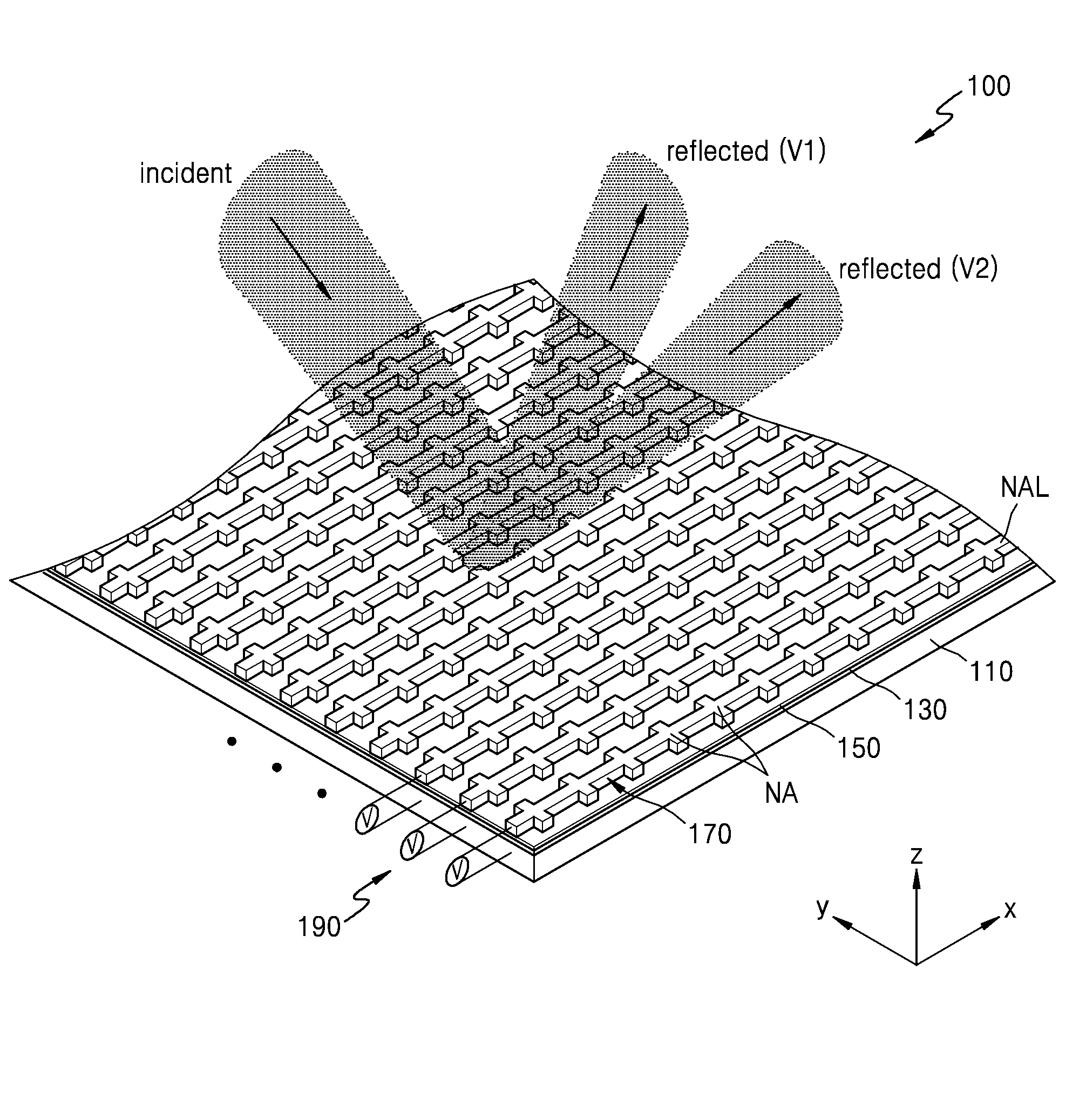
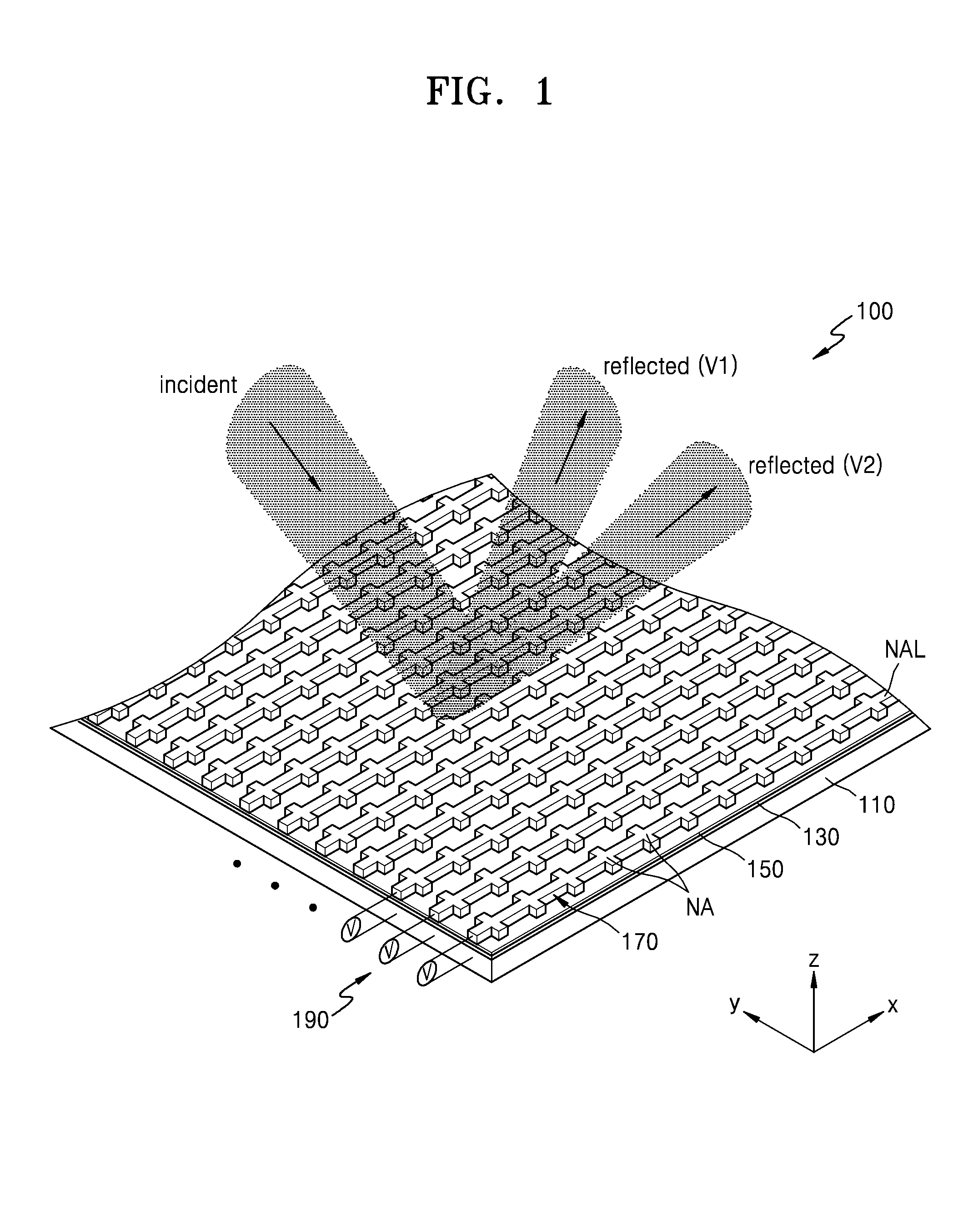
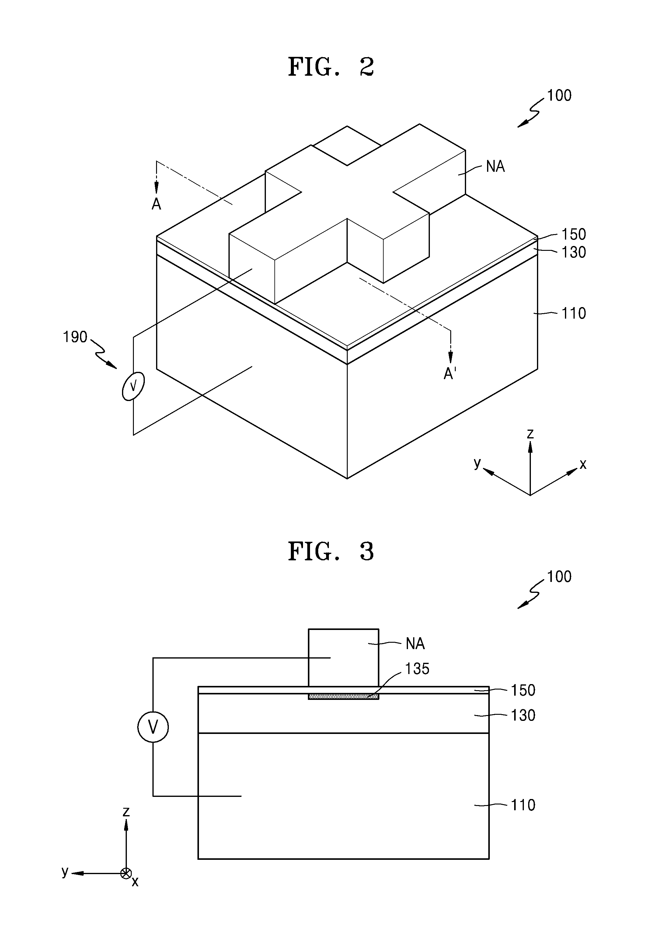
[0053]FIG. 1 is a schematic perspective view of a structure of an optical modulation device 100, according to an exemplary embodiment. FIG. 2 is a detailed perspective view of a unit block of the optical modulatio...


PUM


Abstract

An optical modulation device includes a plasmonic nano-antenna layer, a metal layer that faces the plasmonic nano-antenna layer, and a permittivity variation layer and a dielectric material layer between the plasmonic nano-antenna layer and the metal layer. An active area formed in the permittivity variation layer according to an external signal may function as a gate that controls optical modulation performance.

Description

CROSS-REFERENCE TO RELATED APPLICATION[0001]This application claims the benefit of Korean Patent Application No. 10-2015-0107515, filed on Jul. 29, 2015, in the Korean Intellectual Property Office, and U.S. Provisional Application Ser. No. 62 / 111,583, filed on Feb. 3, 2015, in the United States Patent Trademark Office, the disclosures of which are incorporated herein in their entirety by reference.BACKGROUND[0002]1. Field[0003]Apparatuses consistent with exemplary embodiments relate to optical devices that modulate light.[0004]2. Description of the Related Art[0005]Optical devices that change the transmittance, reflection, polarization, phase, intensity, path, etc. of incident light are utilized in various optical apparatuses. Optical modulators used in optical systems have various structures for controlling these properties in a desired way.[0006]As an example, anisotropic liquid crystals and microelectromechanical system (MEMS) structures, utilizing micromechanical movements to bl...

Claims


Application Information

Patent Timeline
IPC IPC(8): G02B5/00G02F1/19
CPCG02F1/19G02B5/008G02F1/0018G02F1/292G02F2203/10G02F2203/11G02F2203/50
Inventor HAN, SEUNGHOONHUANG, YAO-WEIATWATER, HARRY A.LEE, HO WAISOHKOYAN, RUZANPAPADAKIS, GEORGIATHYAGARAJAN, KRISHNAN
Owner SAMSUNG ELECTRONICS CO LTD
Why Eureka
Try Eureka