Imaging device and electronic device

a technology of electronic devices and imaging devices, applied in the direction of diodes, radiation controlled devices, semiconductor devices, etc., can solve the problems of low illumination conditions, difficult imaging, and decrease in light sensitivity, and achieve low illumination conditions, easy imaging, and high resolution

Inactive Publication Date: 2016-08-04
SEMICON ENERGY LAB CO LTD
View PDF8 Cites 13 Cited by
  • Summary
  • Abstract
  • Description
  • Claims
  • Application Information

AI Technical Summary

Benefits of technology

[0014]An object of one embodiment of the present invention is to provide an imaging device that easily performs imaging under a low illuminance condition. Another object of one embodiment of the present invention is to provide a low-power imaging device. Another object of one embodiment of the present invention is to provide an imaging device that is suitable for high-speed operation. Another object of one embodiment of the present invention is to provide an imaging device with high resolution. Another object of one embodiment of the present invention is to provide a highly integrated imaging device. Another object of one embodiment of the present invention is to provide an imaging device with a wide dynamic range. Another object of one embodiment of the present invention is to provide an imaging device that can be used in a wide temperature range. Another object of one embodiment of the present invention is to provide an imaging device with a high aperture ratio. Another object of one embodiment of the present invention is to provide an imaging device with high reliability. Another object of one embodiment of the present invention is to provide a novel imaging device or the like. Another object of one embodiment of the present invention is to provide a novel semiconductor device or the like.
[0016]One embodiment of the present invention relates to a highly sensitive imaging device that can perform imaging even under a low illuminance condition.
[0021]According to one embodiment of the present invention, an imaging device that easily performs imaging under a low illuminance condition can be provided. A low-power imaging device can be provided. An imaging device that is suitable for high-speed operation can be provided. An imaging device with high resolution can be provided. A highly integrated imaging device can be provided. An imaging device with a wide dynamic range can be provided. An imaging device that can be used in a wide temperature range can be provided. An imaging device with a high aperture ratio can be provided. An imaging device with high reliability can be provided. A novel imaging device or the like can be provided. A novel semiconductor device or the like can be provided.

Problems solved by technology

When the light-receiving area of the photoelectric conversion element is reduced, it might be difficult to perform imaging under a low illuminance condition because of the decrease in sensitivity to light.

Method used


Image

  • Imaging device and electronic device
  • Imaging device and electronic device
  • Imaging device and electronic device

Examples


embodiment 1

[0076]In this embodiment, an imaging device that is one embodiment of the present invention is described with reference to drawings.

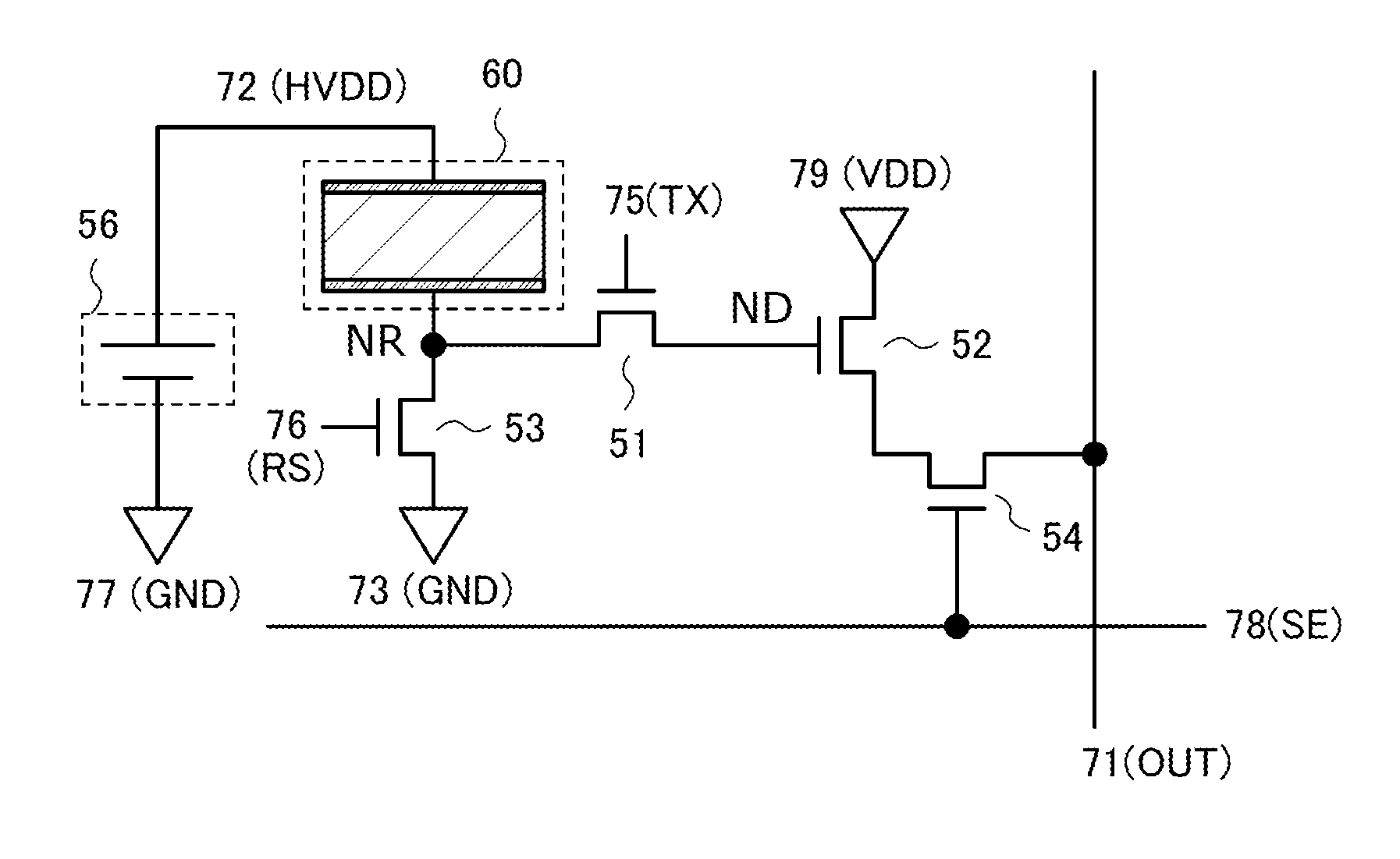
[0077]FIG. 1 illustrates a pixel circuit that can be used for an imaging device in one embodiment of the present invention. The pixel circuit includes a transistor 51, a transistor 52, a transistor 53, a transistor 54, and a photoelectric conversion element 60.

[0078]One electrode of the photoelectric conversion element 60 is electrically connected to one of a source electrode and a drain electrode of the transistor 51. The one electrode of the photoelectric conversion element 60 is electrically connected to one of a source electrode and a drain electrode of the transistor 53. The other of the source electrode and the drain electrode of the transistor 51 is electrically connected to a gate electrode of the transistor 52. One of a source electrode and a drain electrode of the transistor 52 is electrically connected to one of a source electrode and a drain...

embodiment 2

[0181]In this embodiment, a transistor including an oxide semiconductor that can be used in one embodiment of the present invention is described with reference to drawings. In the drawings in this embodiment, some components are enlarged, reduced in size, or omitted for easy understanding.

[0182]FIGS. 24A and 24B are a top view and a cross-sectional view illustrating a transistor 101 in one embodiment of the present invention. FIG. 24A is a top view, and a cross section in the direction of dashed-dotted line B1-B2 in FIG. 24A is illustrated in FIG. 24B. A cross section in the direction of dashed-dotted line B3-B4 in FIG. 24A is illustrated in FIG. 26A. The direction of dashed-dotted line B1-B2 is referred to as a channel length direction, and the direction of dashed-dotted line B3-B4 is referred to as a channel width direction.

[0183]The transistor 101 includes an insulating layer 120 in contact with a substrate 115; an oxide semiconductor layer 130 in contact with the insulating laye...

embodiment 3

[0243]In this embodiment, components of the transistors described in Embodiment 2 are described in detail.

[0244]As the substrate 115, a glass substrate, a quartz substrate, a semiconductor substrate, a ceramic substrate, a metal substrate having a surface subjected to insulation treatment, or the like can be used. The substrate 115 can be a silicon substrate provided with a transistor and / or a photodiode; and an insulating layer, a wiring, a conductor functioning as a contact plug, and the like that are provided over the silicon substrate. Note that when p-channel transistors are formed using the silicon substrate, a silicon substrate with n−-type conductivity is preferably used. Alternatively, an SOI substrate including an n−-type or i-type silicon layer may be used. In the case where a p-channel transistor is formed using the silicon substrate, a surface of the silicon substrate where the transistor is formed preferably has a (110) plane orientation. Forming a p-channel transistor...


PUM


Abstract

A highly sensitive imaging device that can perform imaging even under a low illuminance condition is provided. One electrode of a photoelectric conversion element is electrically connected to one of a source electrode and a drain electrode of a first transistor and one of a source electrode and a drain electrode of a third transistor. The other of the source electrode and the drain electrode of the first transistor is electrically connected to a gate electrode of the second transistor. The other electrode of the photoelectric conversion element is electrically connected to a first wiring. A gate electrode of the first transistor is electrically connected to a second wiring. When a potential supplied to the first wiring is HVDD, the highest value of a potential supplied to the second wiring is lower than HVDD.

Description

BACKGROUND OF THE INVENTION[0001]1. Field of the Invention[0002]One embodiment of the present invention relates to an imaging device including an oxide semiconductor.[0003]Note that one embodiment of the present invention is not limited to the above technical field. The technical field of one embodiment of the invention disclosed in this specification and the like relates to an object, a method, or a manufacturing method. One embodiment of the present invention relates to a process, a machine, manufacture, or a composition of matter. Specifically, examples of the technical field of one embodiment of the present invention disclosed in this specification include a semiconductor device, a display device, a liquid crystal display device, a light-emitting device, a lighting device, a power storage device, a storage device, an imaging device, a method for driving any of them, and a method for manufacturing any of them.[0004]In this specification and the like, a semiconductor device genera...

Claims


Application Information

Patent Timeline
Patent Type & Authority Applications(United States)
IPC IPC(8): H01L27/146H01L29/786
CPCH01L29/7869H01L27/14616H01L27/14627H01L27/14641H01L27/14663H01L27/14665H01L27/14692H01L27/14696H01L27/1207H01L27/1225H01L27/14612H01L27/14636H01L27/14618H01L27/14643
Inventor KUROKAWA, YOSHIYUKI
Owner SEMICON ENERGY LAB CO LTD
Why Eureka
Try Eureka