3D printed chamber components configured for lower film stress and lower operating temperature

a chamber and film stress technology, applied in the field of chamber components, can solve the problems of high film stress of materials, circuit inoperable, and degrade the overall performance of the integrated circuit, and achieve the effect of reducing film stress

Active Publication Date: 2016-08-11
APPLIED MATERIALS INC
View PDF4 Cites 20 Cited by
  • Summary
  • Abstract
  • Description
  • Claims
  • Application Information

AI Technical Summary

Benefits of technology

[0010]In one embodiment, a chamber component for a processing chamber has a body. The body has unitary monolithic construction. The body has a textured surface. The textured surface has a plurality of independent engineered features wherein the engineered features include macro features. The engineered features are configured to reduce film stress and tune the thermal conductivity of the chamber component.

Problems solved by technology

Reliably producing sub-half micron and smaller features is one of the key technology challenges for next generation very large scale integration (VLSI) and ultra large-scale integration (ULSI) of semiconductor devices.
However, as the limits of circuit technology are pushed, the shrinking dimensions of VLSI and ULSI interconnect technology have placed additional demands on processing capabilities.
Capacitive coupling between adjacent metal interconnects may cause cross talk and / or resistance-capacitance (RC) delay which degrades the overall performance of the integrated circuit and may render the circuit inoperable.
Existing chamber components utilized in PVD chambers may have a high temperature differential which causes high film stress for materials that adheres to the components during the operation of the PVD chamber.
The higher film stress may result in flaking of the deposited material during operation of the PVD chamber after the film has reached a critical thickness.
The flaking of the deposited material results in increased of contamination (i.e., particles) of the interior of the PVD chamber which contributes to substrate defects and low yield.
Thus, the high risk of contamination undesirably demands increased frequency for cleaning and maintenance of the PVD chamber.

Method used


Image

  • 3D printed chamber components configured for lower film stress and lower operating temperature
  • 3D printed chamber components configured for lower film stress and lower operating temperature
  • 3D printed chamber components configured for lower film stress and lower operating temperature

Examples


Embodiment Construction

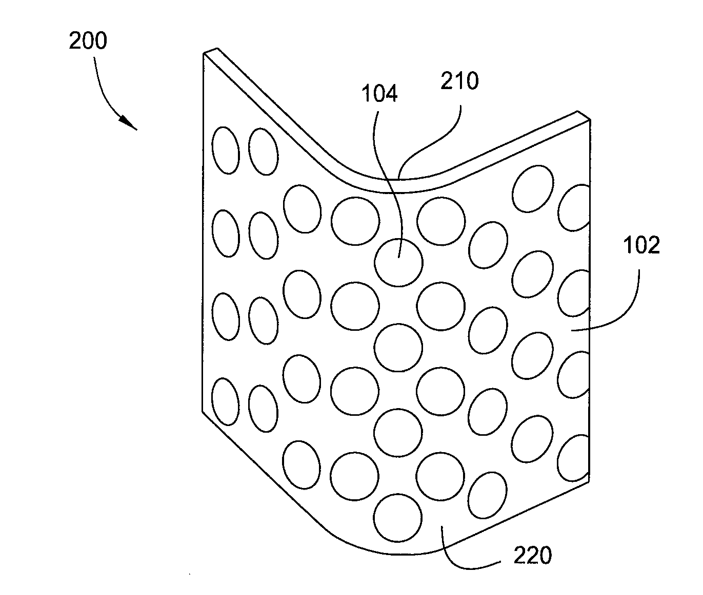
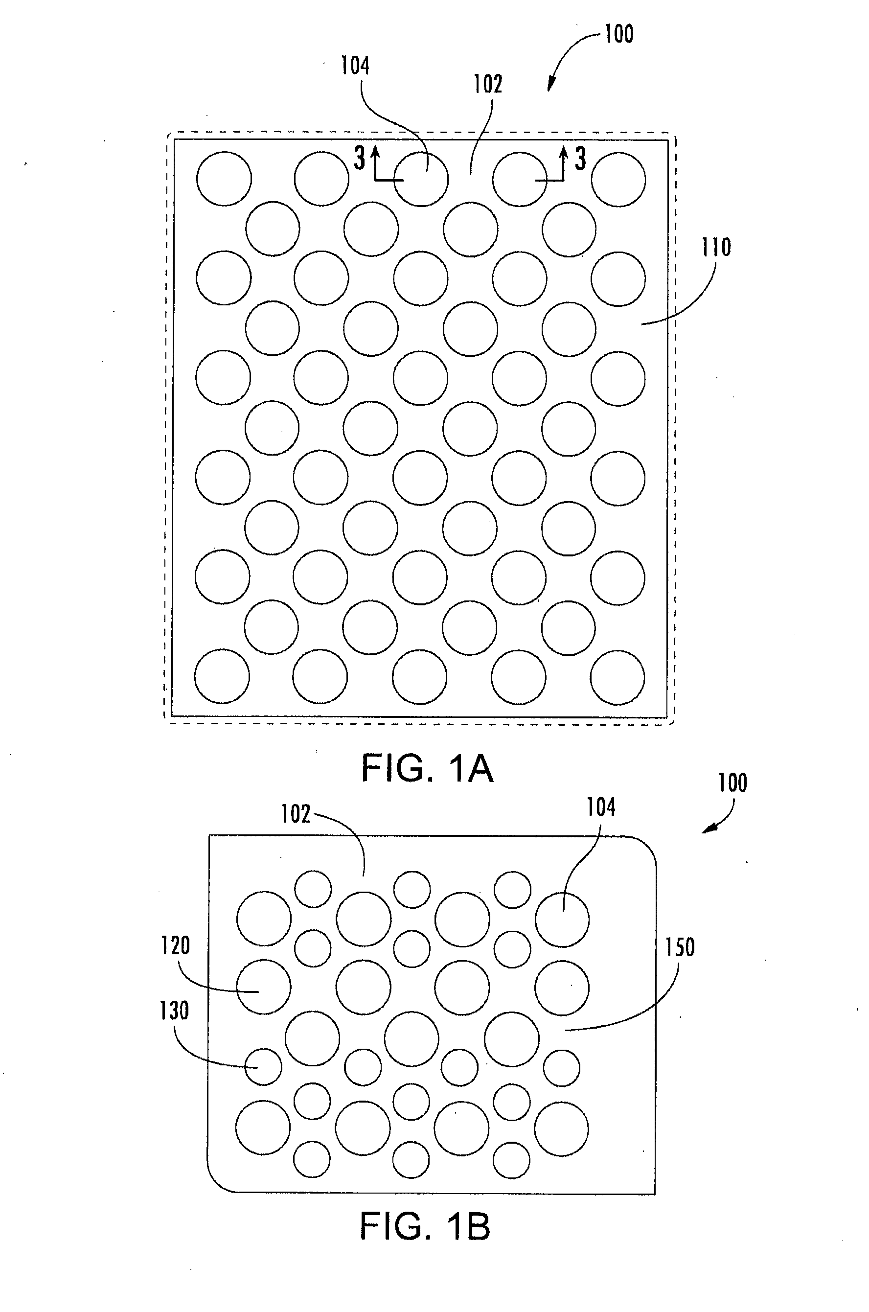
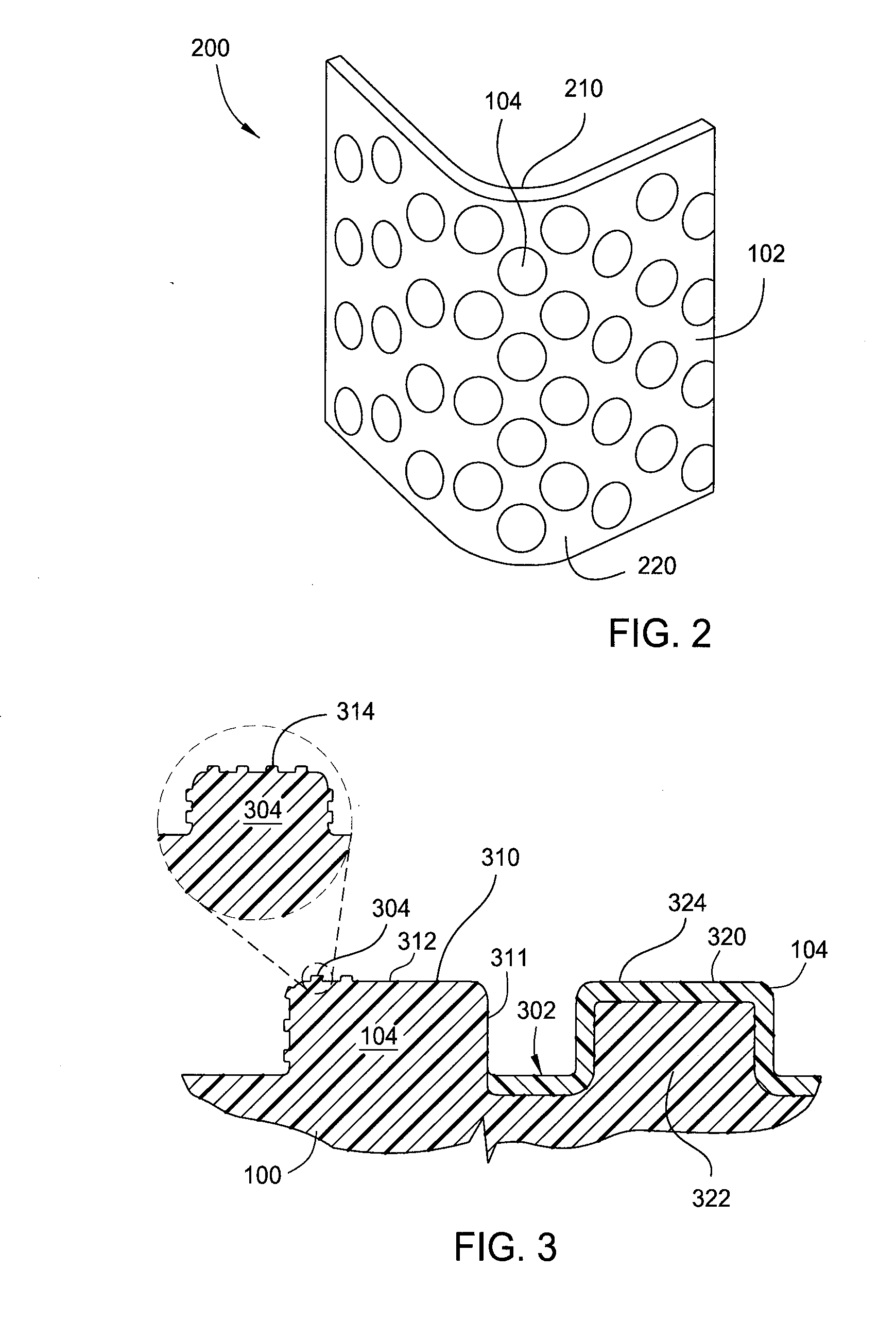
[0029]3D printing is a technique of manufacturing three dimensional components by laying down successive thin layer of material. 3D Printing is also used in Semiconductor industry for manufacturing semiconductor processing chamber components (which include coil cups) for plasma deposition chambers that can provide improved adhesion of deposition material on the surface of the chamber component. In a 3D printing process, a thin layer of precursor, e.g., a powder or other feed stock material is progressively deposited and fused to form a full 3-dimensional component of the chamber. This additive manufacturing technique enables surfaces of the chamber component to be engineered to provide improved film adhesion, which inhibits flaking of the film from the chamber component where the flakes become a process contaminant. This additive manufacturing technique may additionally or alternatively enable surfaces of the chamber components to be engineered to minimize thermal temperature change...


PUM

PropertyMeasurementUnit
widthaaaaaaaaaa
widthaaaaaaaaaa
thicknessaaaaaaaaaa

Abstract

A chamber component for a processing chamber is disclosed herein. In one embodiment, a chamber component for a processing chamber includes a component part body having unitary monolithic construction. The component part body has a textured surface. The textured surface includes a plurality of independent engineered macro features integrally formed with the component part body. The engineered macro features include a macro feature body extending from the textured surface.

Description

CROSS-REFERENCE TO RELATED APPLICATIONS[0001]This application claims benefit of U.S. Provisional Application Ser. No. 62 / 112,649, filed Feb. 6, 2015 (Attorney Docket No. APPM / 22451 USL), and U.S. Provisional Application Ser. No. 62 / 184,114, filed Jun. 24, 2015 (Attorney Docket No. APPM / 22451 USL02), both of which are incorporated by reference in their entirety.BACKGROUND OF THE INVENTION[0002]1. Field of the Invention[0003]Embodiments of the invention relate to chamber components for equipment used in the manufacturing of semiconductor devices[0004]2. Description of the Related Art[0005]Reliably producing sub-half micron and smaller features is one of the key technology challenges for next generation very large scale integration (VLSI) and ultra large-scale integration (ULSI) of semiconductor devices. However, as the limits of circuit technology are pushed, the shrinking dimensions of VLSI and ULSI interconnect technology have placed additional demands on processing capabilities. Re...

Claims


Application Information

Patent Timeline
Patent Type & Authority Applications(United States)
IPC IPC(8): H01J37/32
CPCB33Y80/00H01J37/3211H01J37/32853H01J37/32807H01J37/32477H01J37/32467H01J37/32871H01J37/3288B22F12/70B22F10/18B22F10/14B22F10/32B22F10/25B22F10/28B22F2999/00B22F5/106B22F2005/004B22F2005/005Y02P10/25B33Y10/00B22F3/11
Inventor NARENDRNATH, KADTHALA R.RAJ, GOVINDAYOSHIDOME, GOICHIVASANTHA, BOPANNA ICHETTIRAKELKAR, UMESH M.
Owner APPLIED MATERIALS INC
Why Eureka
Try Eureka