Semiconductor device

a technology of semiconductor devices and semiconductor devices, applied in semiconductor devices, semiconductor/solid-state device details, electrical apparatus, etc., can solve the problems of reducing ic destruction by the esd, and the off transistor cannot exhibit sufficiently, so as to improve the resistance of the semiconductor device to the esd, the parasitic resistance of the output element may be reduced.

Active Publication Date: 2016-08-11
ABLIC INC
View PDF4 Cites 0 Cited by
  • Summary
  • Abstract
  • Description
  • Claims
  • Application Information

AI Technical Summary

Benefits of technology

The invention aims to reduce the parasitic resistance of the off transistor in a semiconductor device, which helps to quickly start its operation and suppress the propagation of electrostatic pulse to an output element or internal circuit element. This improves the resistance of the semiconductor device to electrostatic discharge (ESD).

Problems solved by technology

As a result, the off transistor cannot sufficiently exhibit its performance and an electrostatic pulse originally supposed to be taken by the off transistor may be propagated to the internal circuit element or the output element, resulting in IC destruction by the ESD.
However, in the former case, namely, for attaining high driving performance, there is a fear in that the parasitic resistance of the output element is reduced to be lower than that of an off transistor, with the result that an electrostatic pulse cannot be taken by the off transistor sufficiently, and is propagated to the output element to cause IC destruction.
Moreover, in the latter case, namely, for obtaining high added value, there is a fear in that a parasitic resistance of a source of the off transistor becomes more conspicuous because an IC is large in size and an external connection terminal is located away from a VSS of the IC, with the result that an electrostatic pulse cannot sufficiently be taken by the off transistor, and is propagated to the internal circuit element to cause IC destruction.

Method used


Image

  • Semiconductor device
  • Semiconductor device
  • Semiconductor device

Examples


Embodiment Construction

[0017]A mode for carrying out the present invention is described with reference to the drawings.

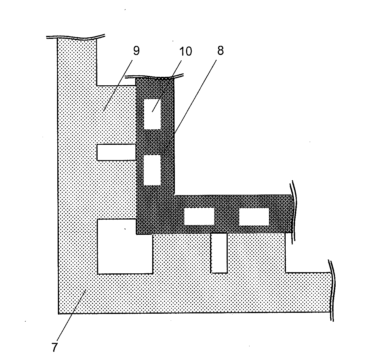
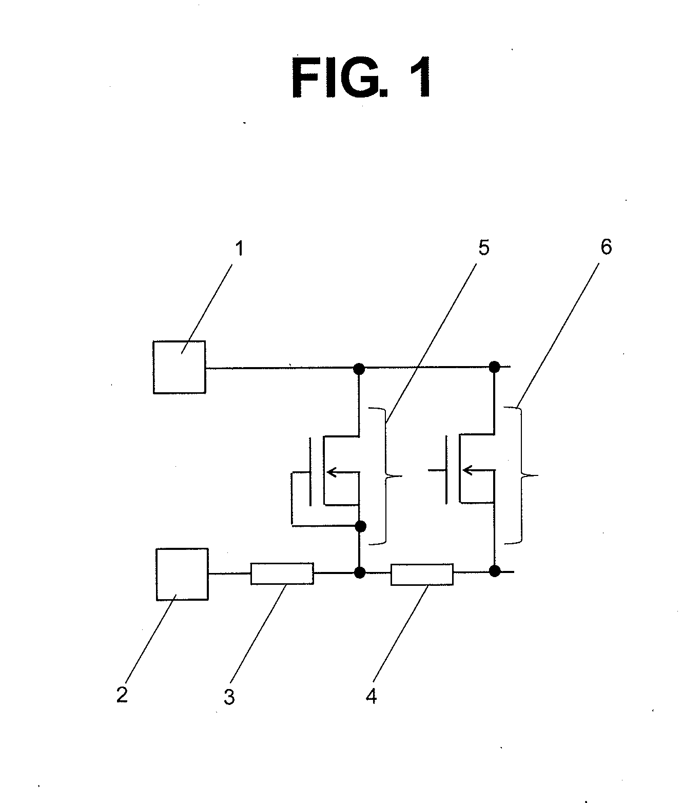
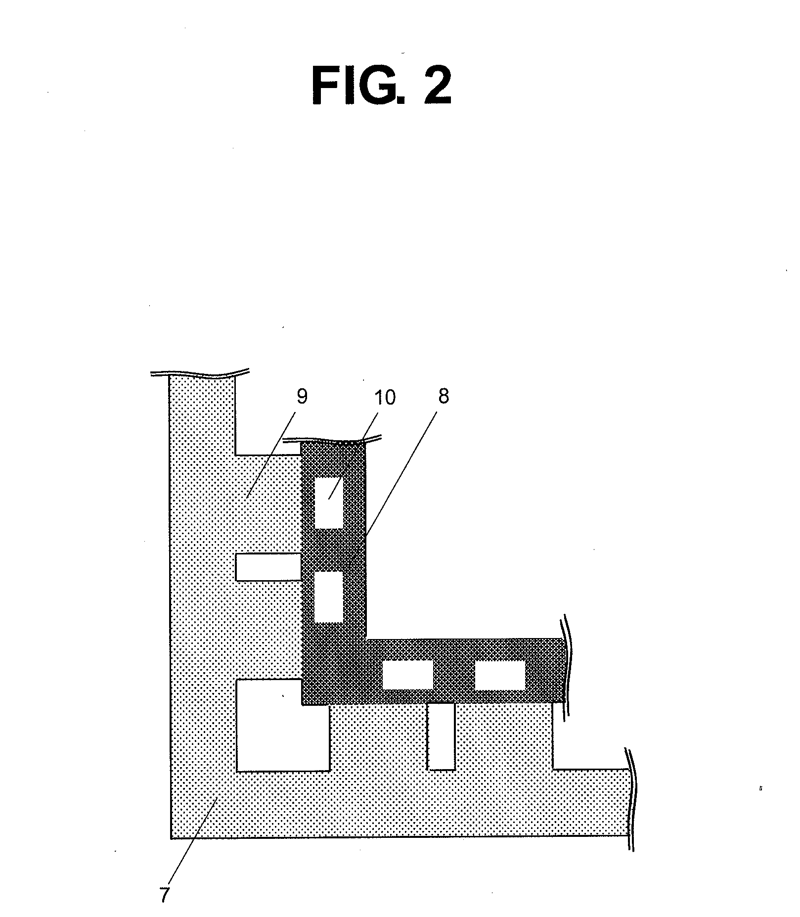
[0018]FIG. 1 is a schematic circuit diagram for illustrating external connection terminals, an ESD protection element, and an output element of a semiconductor device according to the embodiment of the present invention. A first external connection terminal 1 is, for example, a terminal for output. A second external connection terminal 2 has a power supply voltage on a lower side and is generally connected to a ground potential VSS. One of elements connected between the first external connection terminal 1 and the second external connection terminal 2 is an off transistor 5 serving as an ESD protection element. Further, an output element 6 is connected in parallel to the off transistor 5. That is, an output of the output element 6 is connected to the first external connection terminal 1.

[0019]A parasitic resistance of a source of the off transistor 5, which is represented by reference num...


PUM


Abstract

In the semiconductor device including the off transistor serving as an ESD protection element and an output element between a first external connection terminal and a second external connection terminal connected to a VSS, a seal ring wire is connected in parallel, by a connection wire, to a first internal wire extending from the second external connection terminal to the source of the off transistor, and a parasitic resistance of the first internal wire is smaller than a parasitic resistance of a second internal wire connecting the source of the off transistor and a source of the output element to each other.

Description

BACKGROUND OF THE INVENTION[0001]1. Field of the Invention[0002]The present invention relates to a semiconductor device, which includes, in order to protect a semiconductor integrated circuit (hereinafter referred to as “IC”) against destruction due to an electrostatic pulse generated by electrostatic discharge (hereinafter referred to as “ESD”), an ESD protection element formed between an external connection terminal and an internal circuit region, or between the external connection terminal and an output element.[0003]2. Description of the Related Art[0004]Hitherto, semiconductor devices represented by ICs include ESD protection elements, and so-called off transistors are known as the ESD protection elements. The off transistor is an N-type MOS transistor having a gate potential fixed to a ground potential (hereinafter referred to as “VSS”), and thus is in an off state as a steady state.[0005]What is important for an ESD countermeasure is that, in order to prevent ESD destruction ...

Claims


Application Information

Patent Timeline
Patent Type & Authority Applications(United States)
IPC IPC(8): H01L27/02H01L23/535H01L29/06
CPCH01L27/027H01L23/535H01L29/0619H01L27/0266H01L29/78H01L23/5286H01L27/0292
Inventor HASHITANI, MASAYUKIHASEGAWA, HISASHITAKASHINA, TAKAYUKIMASUKO, HIROYUKI
Owner ABLIC INC
Why Eureka
Try Eureka