

Device and method for aligning substrates
a technology of substrates and air bearings, applied in semiconductor/solid-state device testing/measurement, instruments, photomechanical devices, etc., can solve the problems of correspondingly inaccurate positioning of two substrates relative, difficulty in using the above-mentioned air bearings, etc., to achieve a large suppression of errors in the x-direction and/or the y-direction, and improve the packing density of functional units.
- Summary
- Abstract
- Description
- Claims
- Application Information
AI Technical Summary
Benefits of technology
Problems solved by technology
Method used
Image

Examples
Embodiment Construction
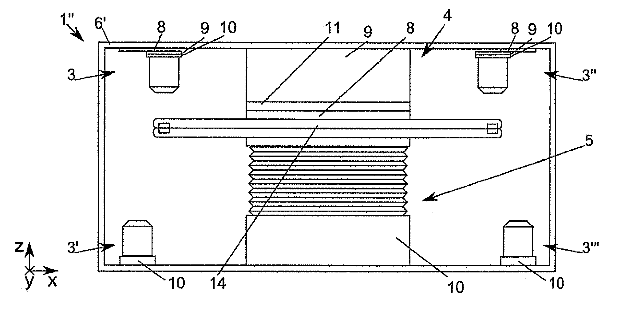
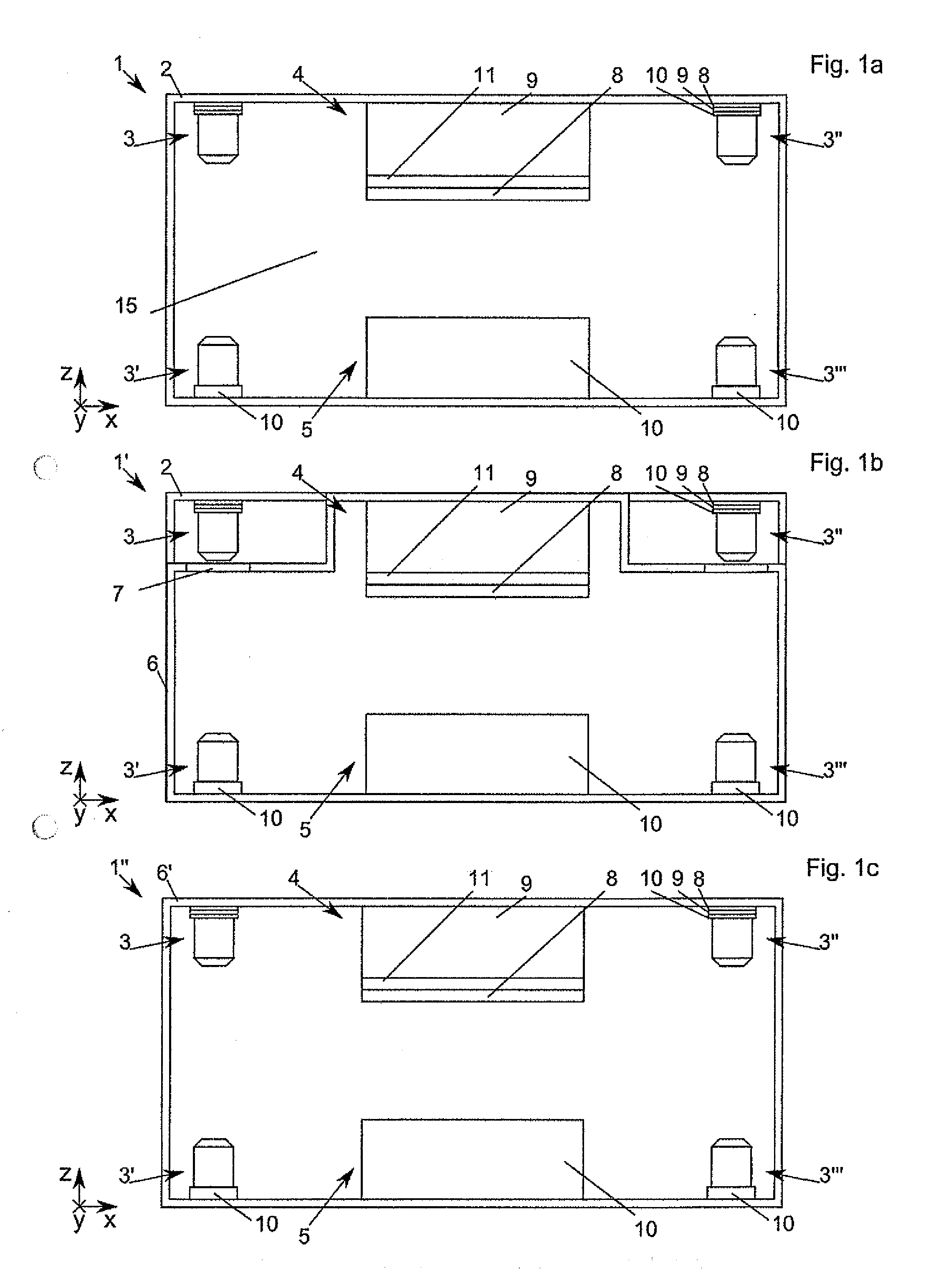
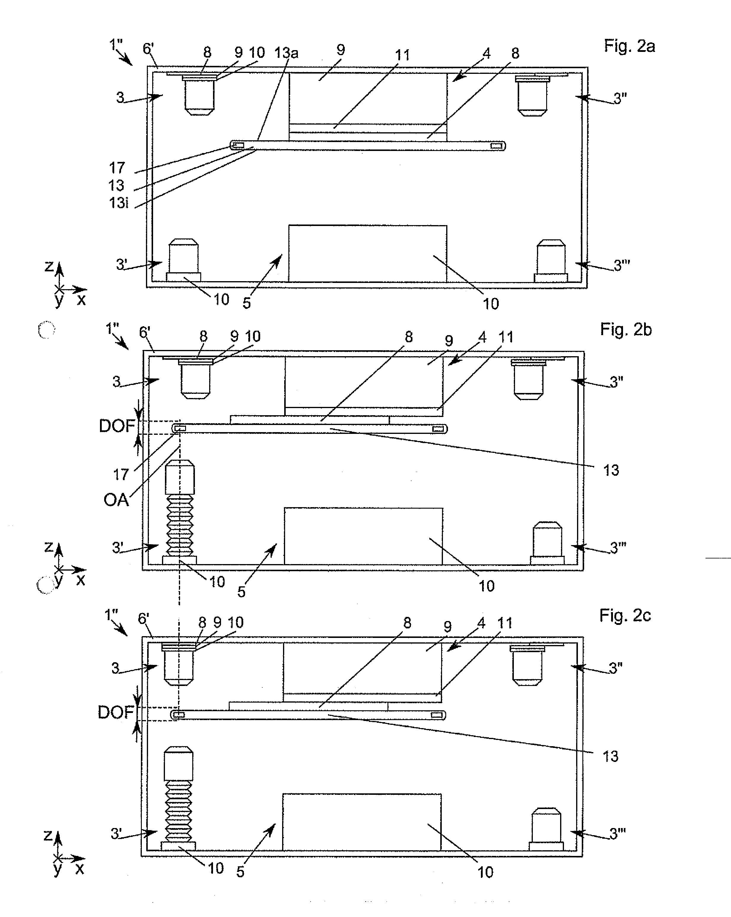
[0160]In the figures, advantages and features of the invention are characterized with these reference numbers to be identified in each case according to embodiments of the invention, whereby components or features with functions that are the same or that have the same effect are characterized with identical reference numbers.
[0161]FIGS. 1a-1c show respectively diagrammatic cross-sections of three embodiments of alignment units 1, 1′, 1″ comprised of:[0162]A first detection unit 3 in the form of a left upper optics or with a left upper optics.[0163]A second detection unit 3′ in the form of a left lower optics or with a left lower optics, as well as[0164]Another first detection unit 3″ in the form of a right upper optics or with a right upper optics, and[0165]Another second detection unit 3′″ in the form of one right lower optics or with one right lower optics,[0166]A first holder 4 in the form of an upper holder or with an upper holder, as well as[0167]A second holder 5 in the form o...
PUM
 Abstract
Description
Claims
Application Information