Display backplane and method of fabricating the same

a backplane and display technology, applied in the direction of semiconductor devices, instruments, electrical apparatus, etc., can solve the problems of increased manufacturing time and cost of display backplanes, difficult high-speed drive circuits for display displays, and display non-uniformity, so as to achieve low power consumption and high resolution

Active Publication Date: 2016-08-18
LG DISPLAY CO LTD
View PDF2 Cites 60 Cited by
  • Summary
  • Abstract
  • Description
  • Claims
  • Application Information

AI Technical Summary

Benefits of technology

[0011]In view of the problems above, inventors of the embodiments in the present disclosure recognized that there is a limit in a conventional TFT backplane employing only one kind TFTs as its constituent TFTs. In recent years, as FPDs have been widely applied to devices requiring versatile pixel driving methods, there is a need for providing a TFT backplane that combines advantages of various types of TFTs such as oxide TFTs and LIPS TFTs. In particular, when various types of TFTs on a substrate are applied to a TFT backplane, a display with high resolution and low power consumption can be provided.

Problems solved by technology

Thus, making a high speed drive circuit (e.g., pixel circuit, gate drive integrated circuit, data drive integrated circuit) for a display is difficult with the TFT backplane employing a-Si TFTs.
Despite significantly high carrier mobility of LIPS TFT, there is a downside as LIPS TFTs of a backplane has variations in their threshold voltages (Vth) due to a grain boundary.
Such non-uniform threshold voltages among the TFTs employed in a TFT backplane may result in display non-uniformity referred to as the “mura.” For this reason, a display drive circuit implemented with LIPS TFTs often requires a complex compensation circuit, which in turn, occurs a problem as it increases the manufacturing time and cost of the display.
However, because lowering the temperature during the fabrication process degrades the performance of the TFTs, there was a limitation in applying the above TFTs to flexible displays.
For example, adopting the etch-stopper type oxide TFTs can improve the reliability, but such a design suffers from high parasitic capacitance and complicates the manufacturing process.
Further, the etch-stopper type limits how short the TFT channel can be, thereby affecting the overall size of the display backplane or the aperture ratio in the pixels of the display.
As such, there are difficulties for designing the driving circuitry for a display.

Method used


Image

  • Display backplane and method of fabricating the same
  • Display backplane and method of fabricating the same
  • Display backplane and method of fabricating the same

Examples


Embodiment Construction

[0044]Various features and advantages described in the present disclosure will be more clearly understood from the following description with reference to the accompanying drawings. The accompanying drawings are merely illustrative and may not be drawn to scale for easier explanation. Also, components having the same or similar function may be denoted by the same reference symbols or numeral throughout the drawings for describing various embodiments. The descriptions of the same or similar components may be omitted.

[0045]It will be understood that when an element as a layer, region or substrate is referred to as being “on” or “over” another element, it can be directly on the other element or intervening elements may also be present. In contrast, when an element is referred to as being “directly on” or “directly over” another element, there are no intervening elements present. It will also be understood that when an element is referred to as being “connected” or “coupled” to another ...


PUM


Abstract

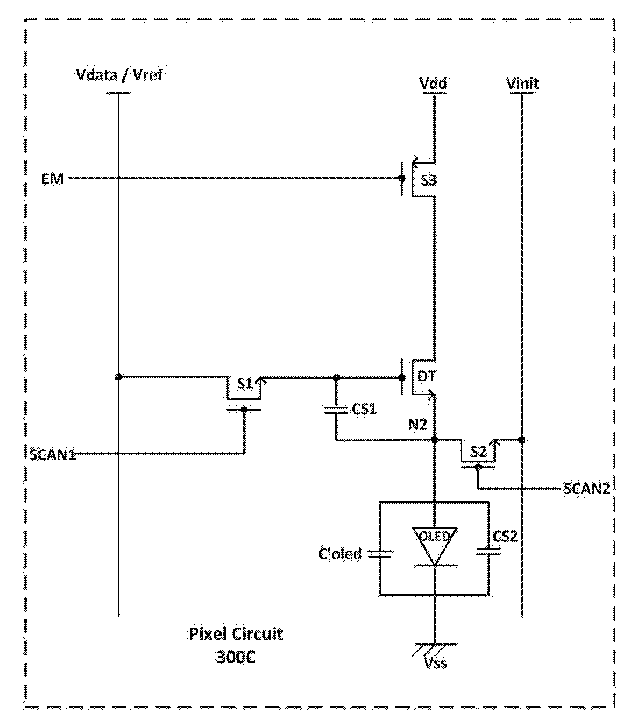
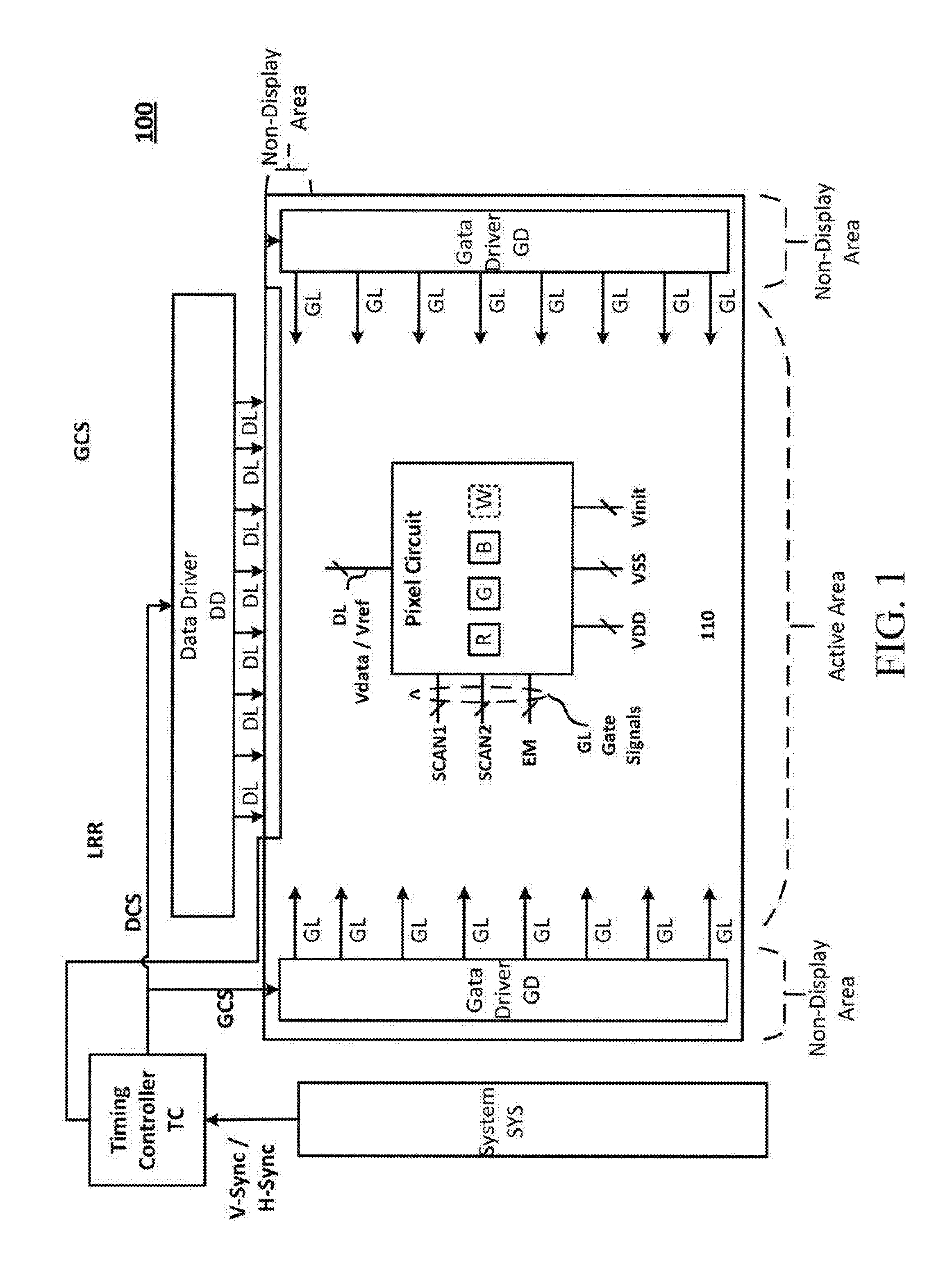
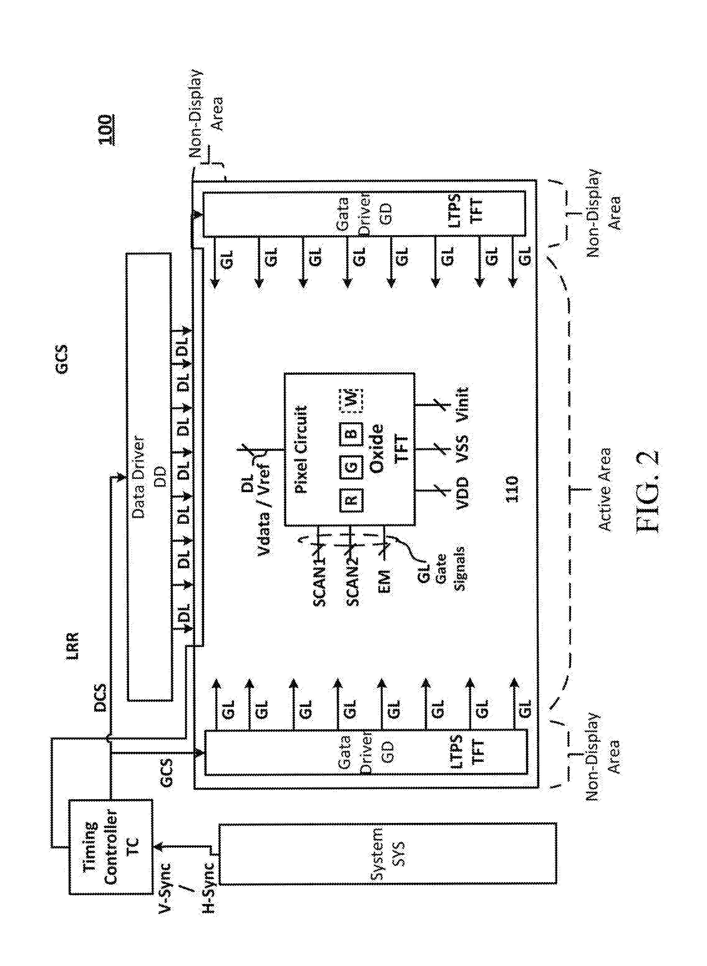
An organic light emitting display is provided. The organic light emitting display comprises a multi-type thin-film transistor (TFT) and an organic light emitting diode. The multi-type TFT has a low-temperature-poly-silicon (LTPS) TFT and an oxide semiconductor TFT (oxide TFT) disposed on the LTPS TFT. The organic light emitting diode is electrically connected to the multi-type TFT. The LTPS TFT and the oxide TFT are connected to the same gate line.

Description

BACKGROUND[0001]1. Technical Field[0002]The present disclosure relates to a thin-film-transistor (TFT) backplane for a display device, and more particularly, to a TFT backplane for more power efficient operation of the display and a method of fabricating such a TFT backplane.[0003]2. Description of the Related Art[0004]Flat panel displays (FPDs) are employed in various electronic devices such as mobile phones, tablets, notebook computers as well as televisions and monitors. Examples of the FPD includes a liquid crystal display (LCD), a plasma display panel (PDP), an organic light emitting diode (OLED) display as well as an electrophoretic display (EPD).[0005]Generally, pixels in a FPD are arranged in a matrix form, and generate light (luminescence) upon electrical activation from an array of thin-film-transistors (TFTs), also known as TFT backplane. A TFT backplane plays an important role in a FPD as it functions as a series of switches to control the current flowing to each individ...

Claims


Application Information

Patent Timeline
Patent Type & Authority Applications(United States)
IPC IPC(8): H01L27/12H01L27/092H01L29/786
CPCH01L27/1251G09G2310/0251H01L27/1225H01L27/124H01L27/1255H01L29/78672H01L29/7869H01L29/78696H01L29/78606H01L27/0922H01L27/3262G09G2300/0408G09G2300/0465G09G2300/0819G09G2300/0852G09G2300/0861H01L27/1222G09G2300/043G09G2300/0452G09G2310/0262G09G3/3233H01L27/0705H10K59/1213
Inventor KIM, TAEHWANCHO, NAMWOOKKIM, HYOUNG-SULEE, JAEMYON
Owner LG DISPLAY CO LTD
Why Eureka
Try Eureka