Display panel and method of fabricating the same

a technology of display panel and aperture ratio, which is applied in the field of display panel, can solve the problems of reducing the area of light transmission region adversely affecting etc., and achieves the effect of avoiding color deviation and improving the aperture ratio of the display panel

Inactive Publication Date: 2016-08-25
AU OPTRONICS CORP
View PDF1 Cites 18 Cited by
  • Summary
  • Abstract
  • Description
  • Claims
  • Application Information

AI Technical Summary

Benefits of technology

[0005]It is therefore one of the objectives of the present disclosure to provide a display panel and a fabrication method thereof to increase aperture ratio and to diminish color deviation.
[0008]The color filters of the display panel of the present disclosure are disposed on the array substrate, and thus the aperture ratio of the display panel is improved. In addition, the TFT devices of the sub-pixel regions configured to display images of different colors are covered with the auxiliary color filter patterns of the same color, and thus all the TFT devices have identical leakage currents and identical device characteristic. Accordingly, color deviation is avoided.

Problems solved by technology

The width incremental of the black matrix, however, reduces the area of light transmission region of the display panel, and thus adversely affects the aperture ratio of the display panel.

Method used


Image

  • Display panel and method of fabricating the same
  • Display panel and method of fabricating the same
  • Display panel and method of fabricating the same

Examples


first embodiment

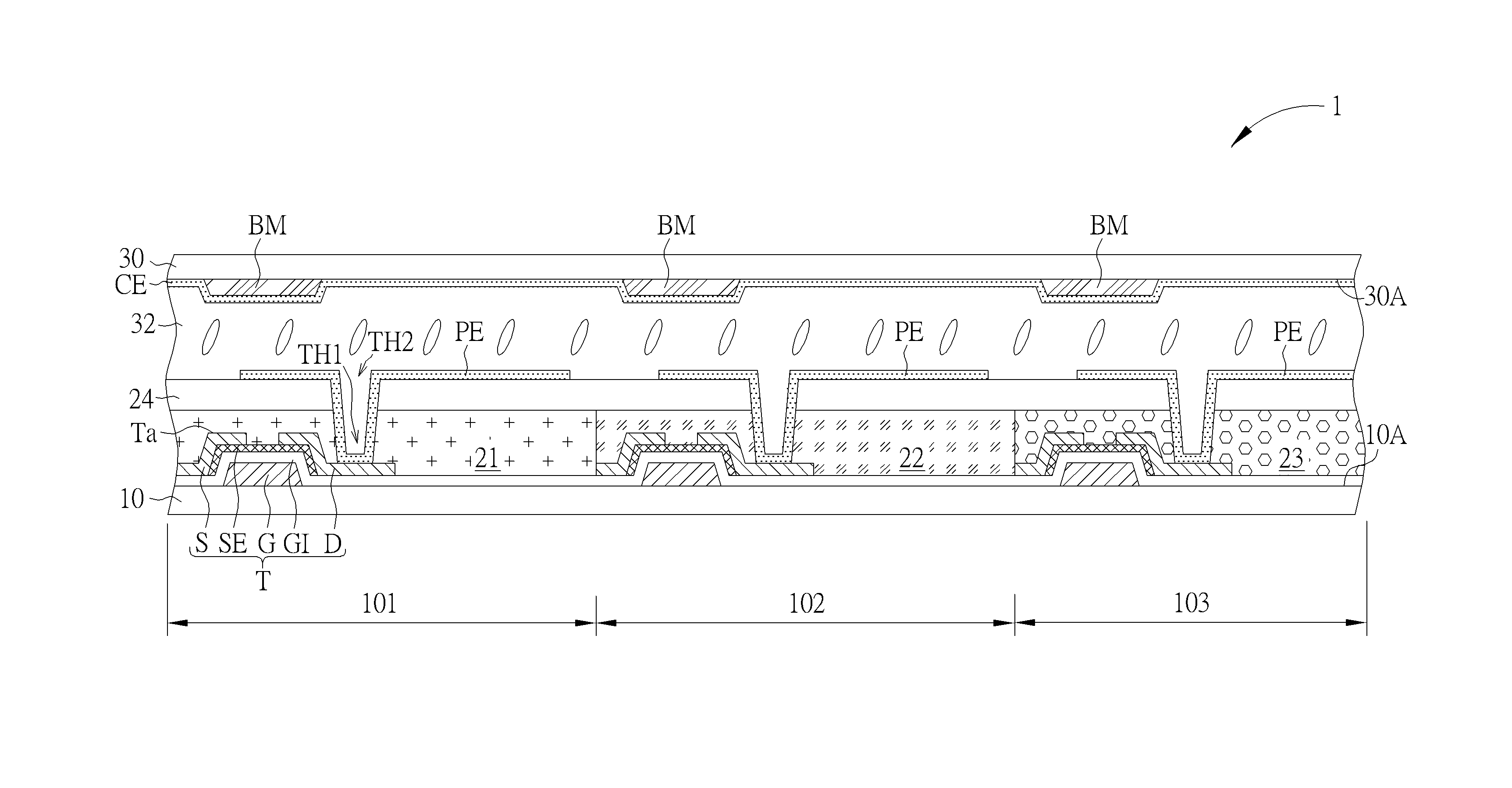
[0022]Refer to FIG. 3. FIG. 3 is a schematic diagram illustrating a display panel according to the present disclosure. As shown in FIG. 3, the display panel 2 of this embodiment is an LCD panel, in which a first substrate 10 may only include two types of sub-pixel regions configured to display images of two different colors. In this embodiment, the sub-pixel regions are first sub-pixel regions 101 and second sub-pixel regions 102. The display panel 2 includes a plurality of TFT devices T, a first color filter 21, a second color filter 22, a plurality of auxiliary color filter patterns 25, a plurality of pixel electrodes PE, a second substrate 30, an opto-electric medium layer 32, a black matrix BM and a common electrode CE. The TFT devices T are disposed on a surface 10A of the first substrate 10 and respectively located in the first sub-pixel region 101 and the second sub-pixel region 102. The TFT device T includes a gate electrode G, a gate insulating layer GI, a semiconductor cha...

second embodiment

[0032]Refer to FIG. 6. FIG. 6 is a schematic diagram illustrating a display panel according to an alternative embodiment of the present disclosure. As shown in FIG. 6, in the display panel 3′ of the alternative embodiment, the light transmission spectrum of the auxiliary color filter patterns 25 is different from the light transmission spectrum of the first color filter 21, the light transmission spectrum of the second color filter 22 and the light transmission spectrum of the third color filter 23. For example, the light transmission wavelength of the auxiliary color filter patterns 25 is preferably longer than the light transmission wavelength of the first color filter 21, the light transmission wavelength of the second color filter 22 and the light transmission spectrum of the third color filter 23. Accordingly, the leakage currents and device characteristic of the TFT devices T are identical, and color deviation is avoided.

[0033]Refer to FIG. 7. FIG. 7 is a schematic diagram ill...


PUM

PropertyMeasurementUnit
light transmission spectraaaaaaaaaaa
light transmission spectrumaaaaaaaaaa
light transmission wavelengthaaaaaaaaaa

Abstract

A display panel and a fabrication method thereof are provided. The display panel includes a substrate, a plurality of thin film transistor devices, color filters having different colors and a plurality of auxiliary color filter patterns. The thin film transistor devices and the color filters are disposed in corresponding pixel regions of the substrate, and each color filter layer has an opening uncovering one corresponding thin film transistor device. The auxiliary color filter patterns are respectively disposed in the openings of the color filter layers, and the auxiliary color filter patterns have the same light transmission spectrum.

Description

BACKGROUND OF THE INVENTION[0001]1. Field of the Invention[0002]The present invention relates to a display panel and method of fabricating the same, and more particularly, to a display panel with high aperture ratio and low color deviation and method of fabricating the same.[0003]2. Description of the Prior Art[0004]Display panel e.g. liquid crystal display (LCD) panel is normally assembled by an array substrate and a color filter substrate (CF substrate). The array substrate includes thin film transistor (TFT) devices and peripheral circuit disposed thereon, and the CF substrate includes color filters e.g. red color filters, green color filters and blue color filters formed thereon. Considering the orientation shift between the array substrate and the CF substrate in assembly process, the width of black matrix must be enlarged to shield light leakage. The width incremental of the black matrix, however, reduces the area of light transmission region of the display panel, and thus adv...

Claims


Application Information

Patent Timeline
Patent Type & Authority Applications(United States)
IPC IPC(8): G02F1/1335H01L27/12G02F1/1343H04N9/12G02F1/1368
CPCG02F1/133516H04N9/12G02F1/1368G02F1/134309G02F2001/134345H01L27/1214H01L27/1262G02F2001/136222G02F1/133512G02F1/1333G02F1/133514G02F1/1362G02F1/133357G02F1/136222
Inventor CHEN, YAO-MINGSHEN, PO-YUANCHEN, CHIA-FANG
Owner AU OPTRONICS CORP
Why Eureka
Try Eureka