

Micro-Electron Column Having An Electron Emitter Improving The Density Of An Electron Beam Emitted From A Nano Structure Tip
- Summary
- Abstract
- Description
- Claims
- Application Information
AI Technical Summary
Benefits of technology
Problems solved by technology
Method used
Image

Examples
first embodiment
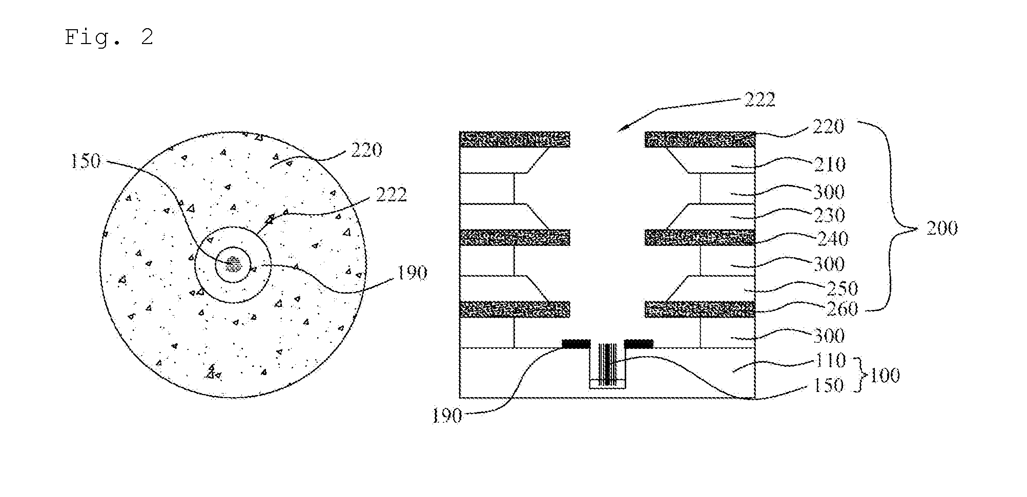
[0032]FIG. 2 illustrates an example of a use of a micro-electron column having nanostructure tips according to the present invention, wherein the left drawing of FIG. 2 is a plane view illustrating a state where the nanostructure tips are disposed at the bottom of the micro-electron column, and the right drawing is a sectional view illustrating the same.
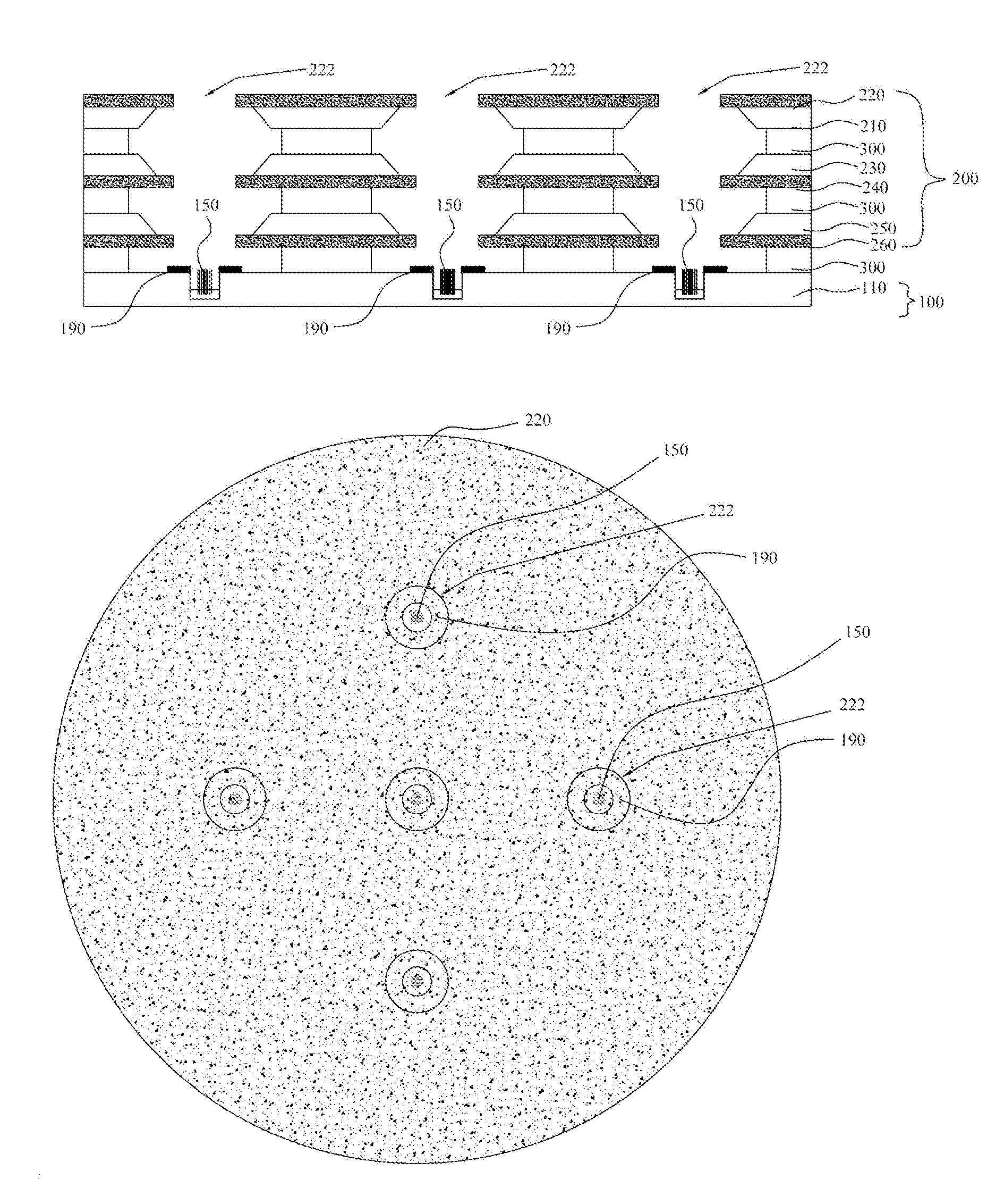
[0033]As shown in FIG. 2, the micro-electron column according to the first embodiment of the present invention is configured such that a source lens 200 is aligned on an electron emitter 100 having a plurality of nanostructure tips 150. An induction electrode 190 is provided at a location adjacent to the end of the nanostructure tips 150. As shown in FIG. 2, the induction electrode 190 may have the same structure and shape as a typical electrostatic lens electrode. However, features of the induction electrode 190, such as external diameter, aperture, or thickness, are determined based on the nanostructure tips 150, unlike the apertur...
second embodiment
[0040]FIG. 4 illustrates plane and sectional views of the micro-electron column having nanostructure tips according to the present invention. In comparison with the micro-electron column of FIG. 2, the micro-electron column of FIG. 4 is configured such that the induction electrode 190 disposed between the electron emitter 100 and the source lens 200 is divided into four pieces. The induction electrode 190 efficiently induces the electrons emitted from the nanostructure tips 150 to enter the aperture 222 of the source lens 200, and also is capable of realigning a direction of an electron beam. The induction electrode 190 may be arrayed with a larger aperture than the aperture 222 of the source lens 200. However, in FIG. 4, the aperture of the induction electrode 190 is smaller in size than the aperture 222 of the source lens as in FIG. 2. The induction electrode 190 may be formed to have four electrode pieces 190a, 190b, 190c, and 190d. The induction electrode 190, however, may have ...
PUM
 Abstract
Description
Claims
Application Information