

Semiconductor device and method for manufacturing same
- Summary
- Abstract
- Description
- Claims
- Application Information
AI Technical Summary
Benefits of technology
Problems solved by technology
Method used
Image

Examples
first embodiment
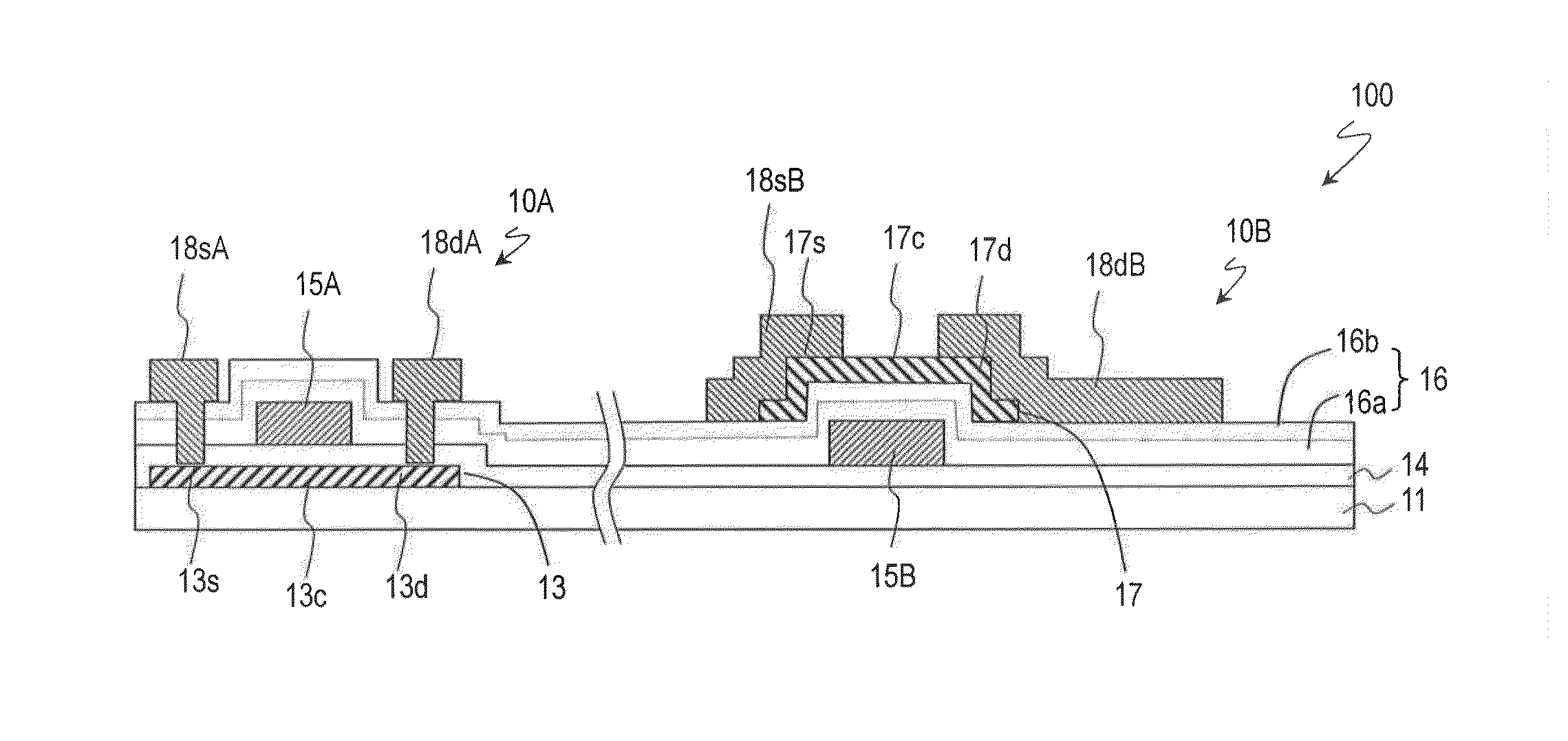
[0057]Hereinafter, a first embodiment of a semiconductor device according to the present invention will be described. The semiconductor device of the present embodiment may at least include crystalline oxide semiconductor TFTs and crystalline silicon TFTs which are formed on the same substrate, and broadly encompasses circuit boards, e.g., active matrix substrates, various display devices, e.g., liquid crystal display devices and organic EL display devices, image sensors, electronic appliances, and the like.
[0058]FIG. 1 is a schematic cross-sectional view of the semiconductor device 100, showing a cross-sectional structure of a crystalline silicon TFT (hereinafter, referred to as a “first thin film transistor”) 10A and a crystalline oxide semiconductor TFT (hereinafter referred to as a “second thin film transistor”) 10B in the semiconductor device 100.
[0059]The semiconductor device 100 includes a substrate 11, the first thin film transistor 10A supported on the substrate 11, and the...
second embodiment
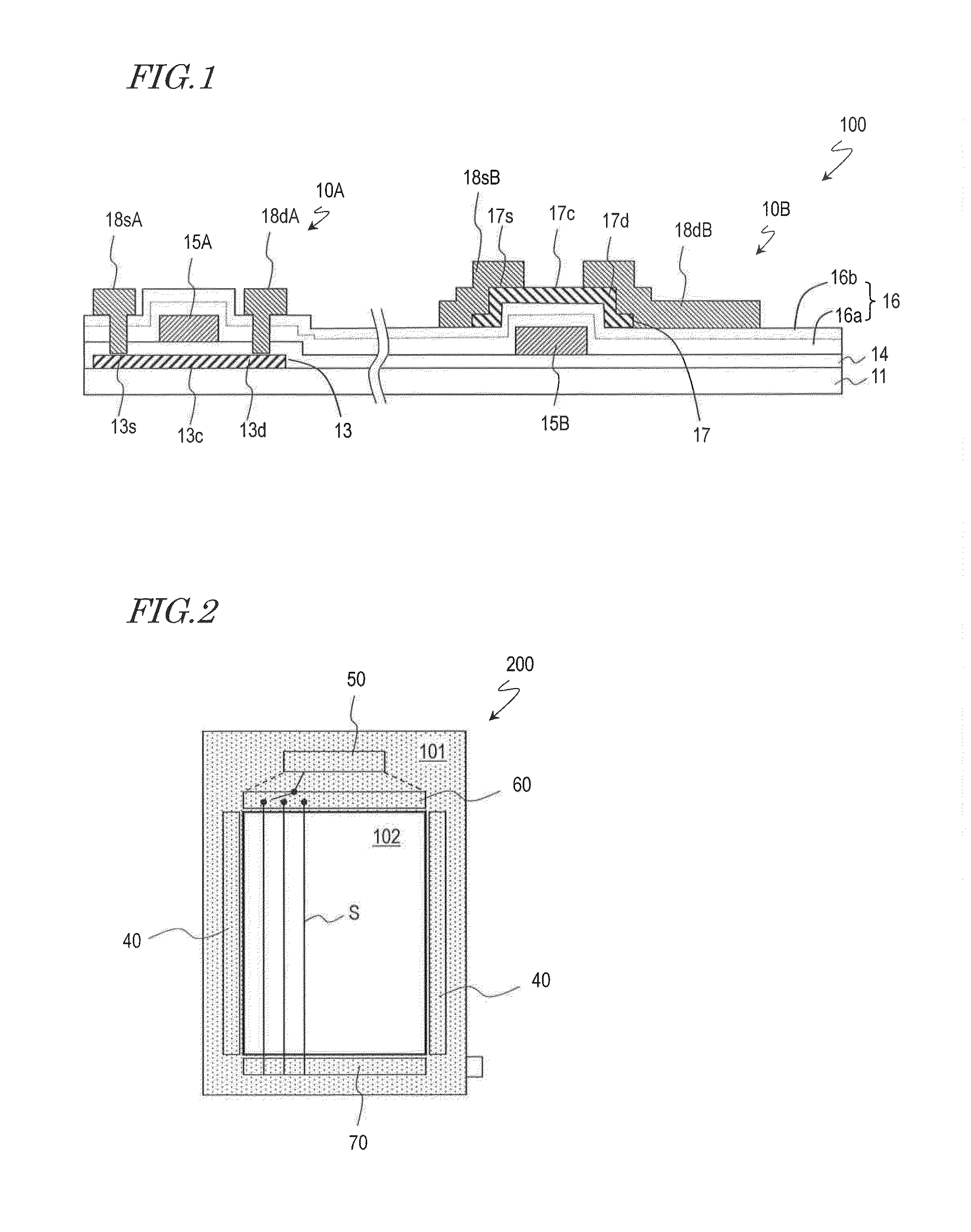
[0111]Hereinafter, a second embodiment of a semiconductor device according to the present invention will be described by taking an active matrix substrate of a display device as an example.
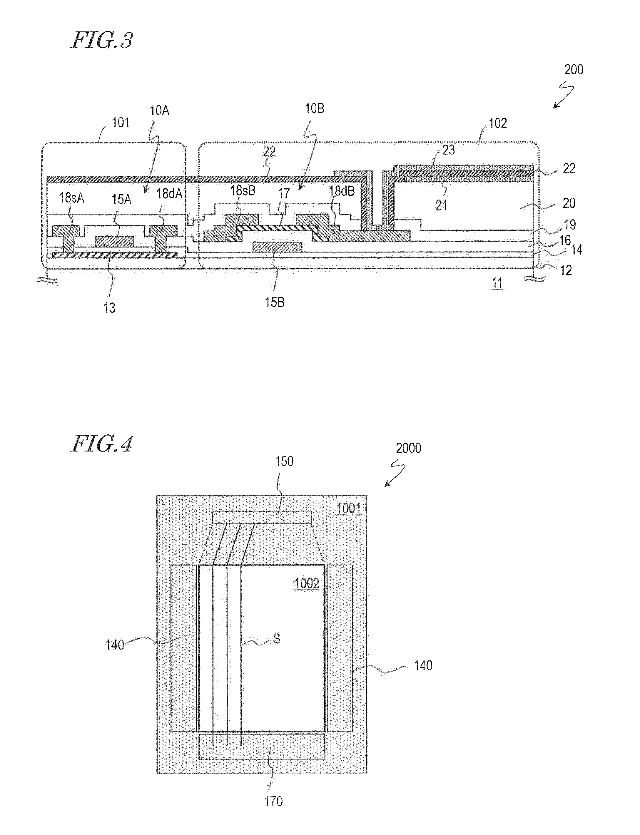
[0112]FIG. 8 is a cross-sectional view illustrating an active matrix substrate 300 according to the present embodiment. The active matrix substrate 300 includes first thin film transistors 10A which are crystalline silicon TFTs and second thin film transistors 10B which are crystalline oxide semiconductor TFTs. In the active matrix substrate 300, the pattern of the crystalline oxide semiconductor layer 17 of the second thin film transistors 10B is made smaller than that of the active matrix substrate 200 of the first embodiment shown in FIG. 3. Moreover, a pixel electrode structure which is different from the active matrix substrate 200 is adopted. Otherwise, the construction is similar to that of the active matrix substrate 200, and the description thereof will be omitted.
[0113]As shown in FIG. 8...
PUM
 Abstract
Description
Claims
Application Information