
Eureka
For R&D, Eureka makes reading and utilizing patents & technical documents easy.
Eureka AIR
Designed for self-driven R&D workflows. Generate viable solutions, solve complex R&D challenges, empower your innovation with AI.

Eureka Materials
Designed for material experts only. Revolutionize your material R&D, from search, analyze, to developing new materials.

TechResearch
Generate reliable direction feasibility study reports for your R&D in just a few steps.

TechSeek
Discover and master advanced knowledge NOW. Basics, ideas, possibilities, all at once.

TechMind
As an expert in R&D Theories, TechMind can generates customized viable solutions instantly.

TechRisk
Analyze your overall solution with one click, know your potential R&D risks in advance.

TechMonitor
Get weekly tech updates, stay abreast of the latest tech innovations and key insights.
Light-emitting element, light-emitting device, electronic device, and lighting device
- Summary
- Abstract
- Description
- Claims
- Application Information
AI Technical Summary
Benefits of technology
Problems solved by technology
Method used
Image

Examples
embodiment 1
[0055]In this embodiment, a light-emitting element of one embodiment of the present invention will be described with reference to FIGS. 1A and 1B, FIGS. 2A and 2B, FIGS. 3A and 3B, FIGS. 4A and 4B, FIG. 5, FIG. 6, and FIG. 7.
1 of Light-Emitting Element>
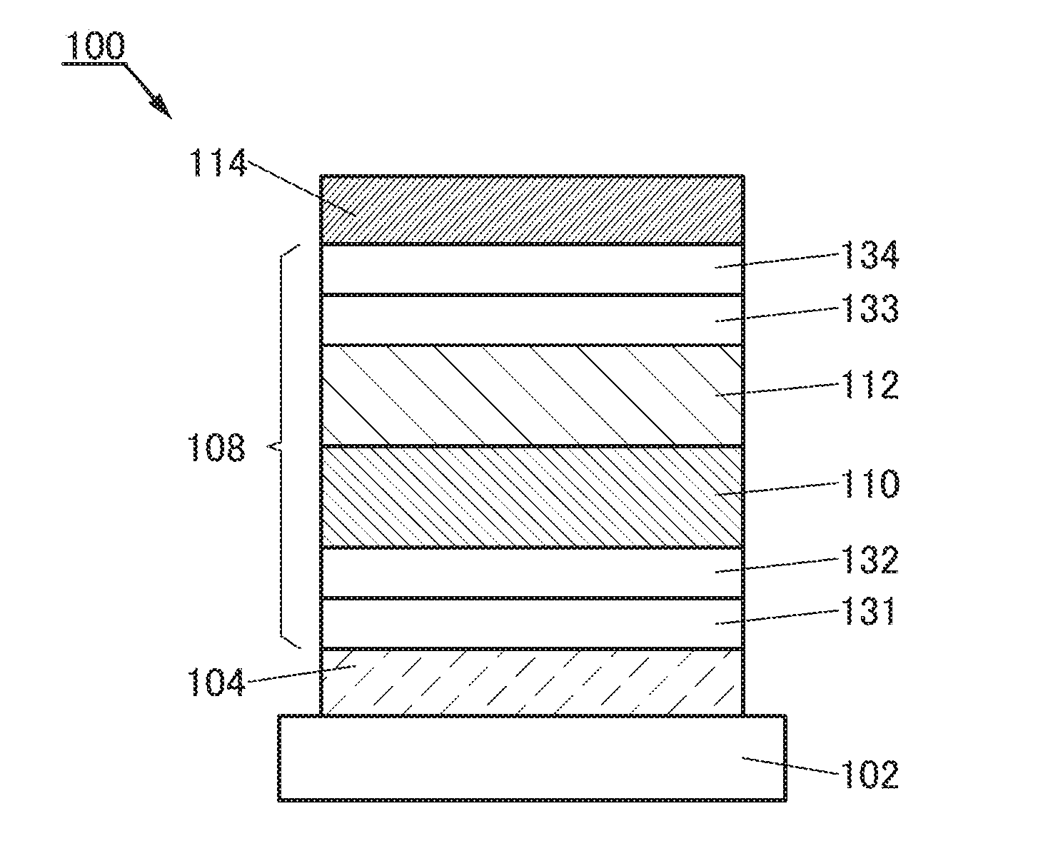
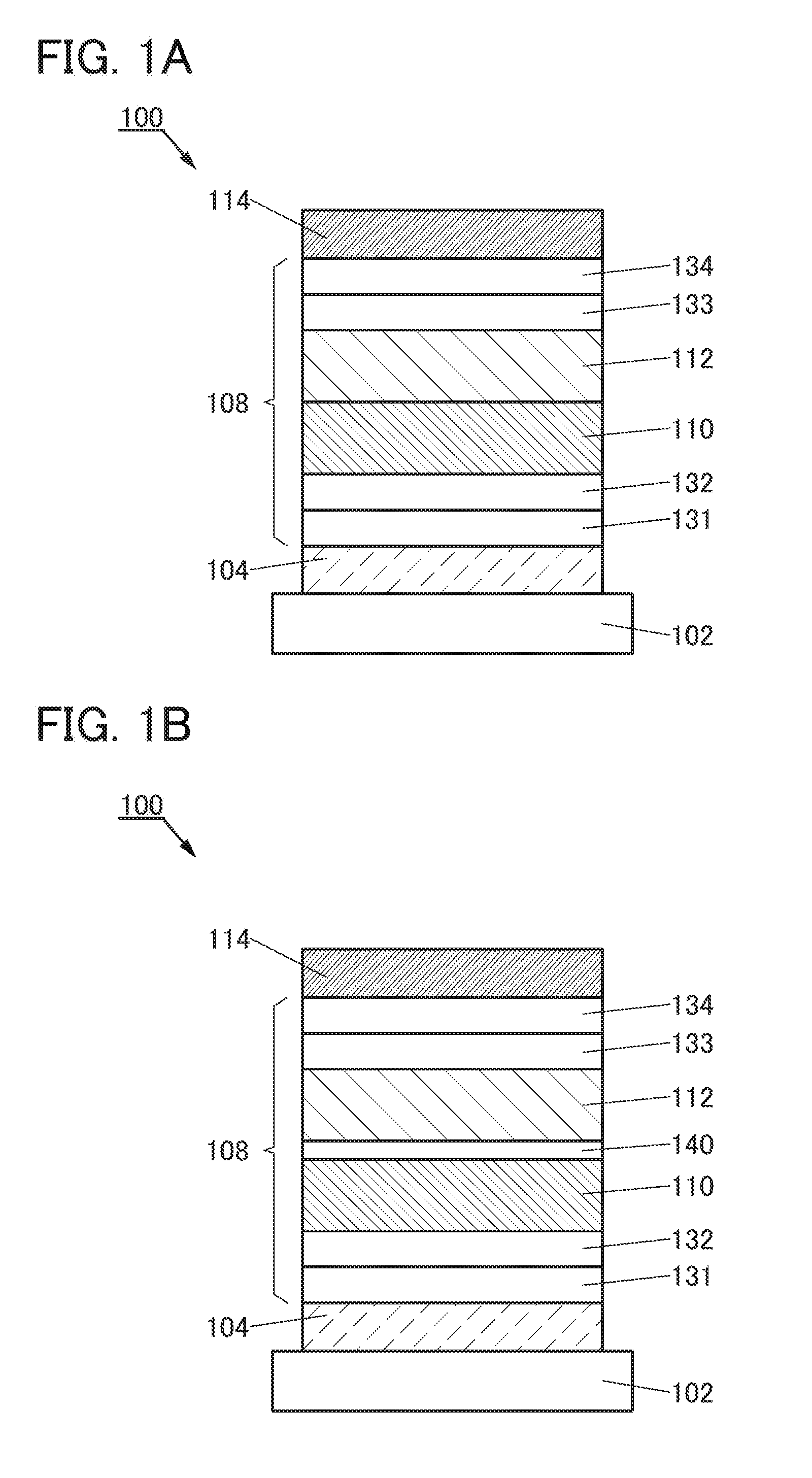
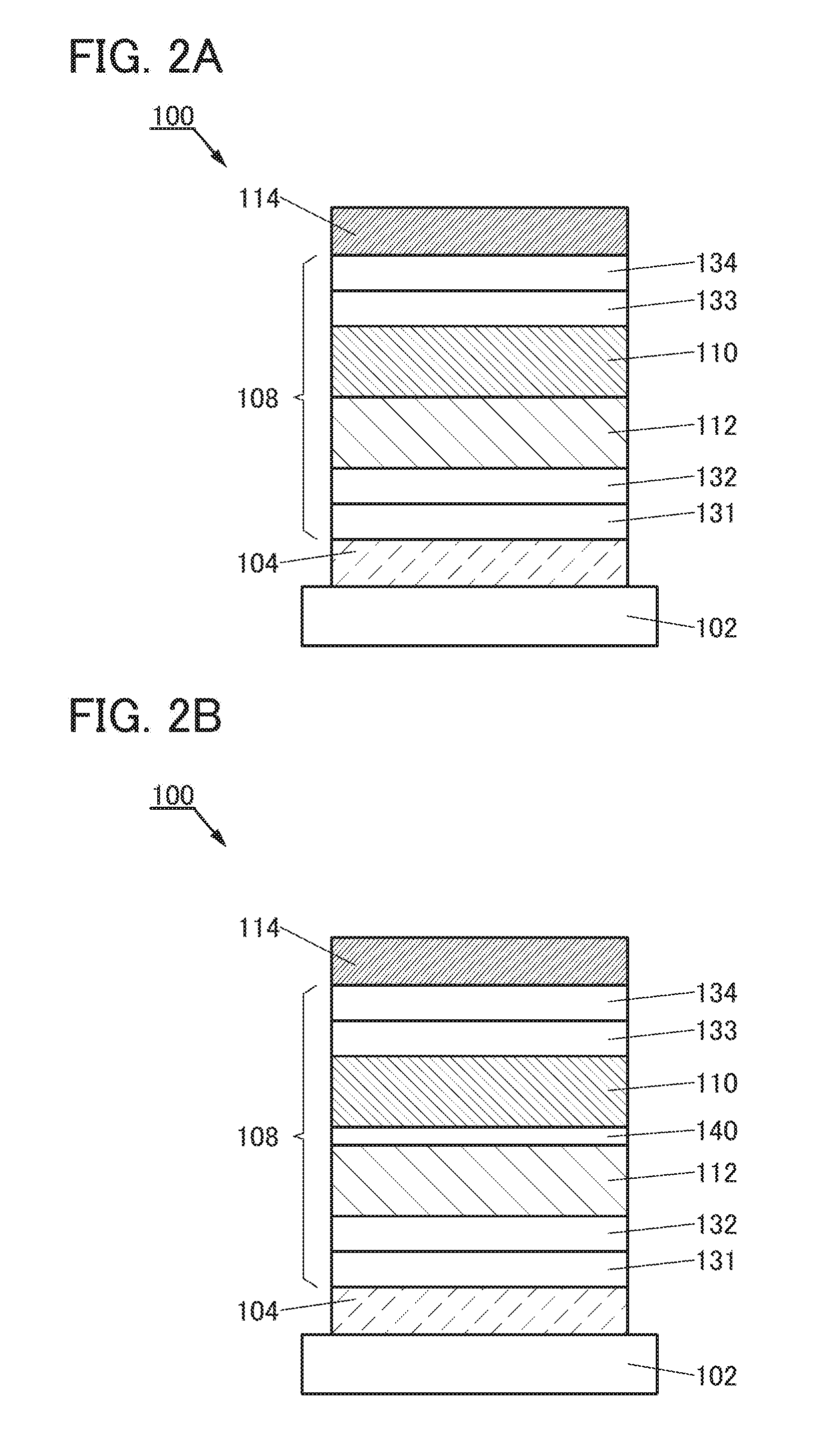
[0056]FIGS. 1A and 1B are schematic cross-sectional views of a light-emitting element 100 of one embodiment of the present invention.
[0057]The light-emitting element 100 illustrated in FIG. 1A includes a first light-emitting layer 110 and a second light-emitting layer 112 between a first electrode 104 and a second electrode 114. The light-emitting element 100 in FIG. 1A further includes a hole-injection layer 131, a hole-transport layer 132, an electron-transport layer 133, and an electron-injection layer 134, in addition to the first light-emitting layer 110 and the second light-emitting layer 112.
[0058]More specifically, the light-emitting element 100 includes the first electrode 104 over a substrate 102, the hole-injection layer 13...
embodiment 2
[0152]In this embodiment, an emission mechanism of the light-emitting element 100 described in Embodiment 1 will be described with reference to FIGS. 8A and 8B, FIGS. 9A and 9B, and FIGS. 10A and 10B.
[0153]First, an emission mechanism of the light-emitting element 100 will be described.
[0154]In the light-emitting element 100 of one embodiment of the present invention, voltage application between a pair of electrodes (the first electrode 104 and the second electrode 114) causes electrons and holes to be injected from the cathode and the anode, respectively, into the EL layer 108 and thus current flows. By recombination of the injected electrons and holes, a guest material (a fluorescent material and a phosphorescent material) in the first light-emitting layer 110 and the second light-emitting layer 112 is brought into an excited state to provide light emission.
1 of First Light-Emitting Layer>
[0155]Next, an emission mechanism of the first light-emitting layer 110 of the light-emitting...
embodiment 3
[0248]In this embodiment, a light-emitting element of one embodiment of the present invention will be described with reference to FIG. 11, FIG. 12, and FIG. 13. Note that FIG. 11 is a schematic cross-sectional view of a light-emitting element 150 of one embodiment of the present invention, and FIG. 12 and FIG. 13 are schematic cross-sectional views of a light-emitting element 150A of one embodiment of the present invention.
2 of Light-Emitting Element>
[0249]The light-emitting element 150 illustrated in FIG. 11 includes a plurality of EL layers (a first EL layer 141 and a second EL layer 142) between the first electrode 104 and the second electrode 114. One or both of the first EL layer 141 and the second EL layer 142 have the same structure as the EL layer 108 illustrated in FIGS. 1A and 1B. That is, the light-emitting element 100 in FIGS. 1A and 1B includes one EL layer while the light-emitting element 150 includes the plurality of EL layers. Note that in this specification and the ...
PUM
 Abstract
Description
Claims
Application Information
 - R&D Engineer
- R&D Manager
- IP Professional
- Industry Leading Data Capabilities
- Powerful AI technology
- Patent DNA Extraction
Browse by: Latest US Patents, China's latest patents, Technical Efficacy Thesaurus, Application Domain, Technology Topic, Popular Technical Reports.
© 2024 PatSnap. All rights reserved.Legal|Privacy policy|Modern Slavery Act Transparency Statement|Sitemap|About US| Contact US: help@patsnap.com