Pixel electrode layer, array substrate, and display panel
- Summary
- Abstract
- Description
- Claims
- Application Information
AI Technical Summary
Benefits of technology
Problems solved by technology
Method used
Image


Examples
Embodiment Construction
[0023]A clear and complete description will be given to technical solutions of the embodiments of the present invention with reference to the attached drawings of the embodiments of the present invention.
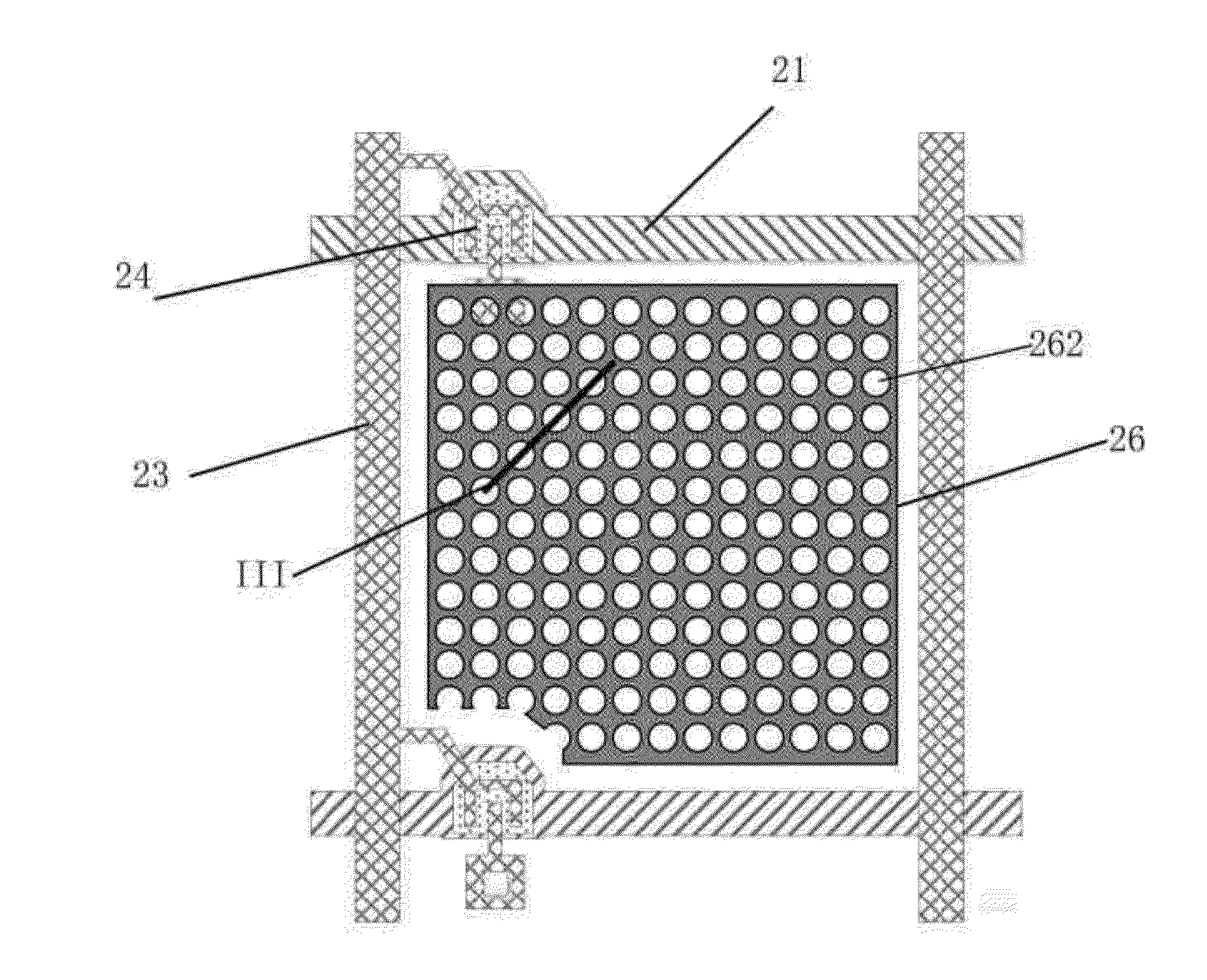
[0024]Referring to FIG. 1, the present invention provides a pixel electrode layer 26. The pixel electrode layer 26 is transparent or semitransparent film. The pixel electrode layer 26 comprises a plurality of circular holes 262 formed therein and the plurality of circular holes 262 causes liquid crystal molecules to be distributed and oriented in a circular form so as to achieve an effect of full view angle.
[0025]The present invention is structured in such a way that the pixel electrode layer 26 is provided with a plurality of circular holes 262 formed therein so that the plurality of circular holes 262 makes liquid crystal molecules distributed and oriented in a circular form to achieve an effect of full view angle. Further, the arrangement of the circular holes 262 that helps achi...
PUM
 Abstract
Description
Claims
Application Information
 - R&D
- Intellectual Property
- Life Sciences
- Materials
- Tech Scout
- Unparalleled Data Quality
- Higher Quality Content
- 60% Fewer Hallucinations
Browse by: Latest US Patents, China's latest patents, Technical Efficacy Thesaurus, Application Domain, Technology Topic, Popular Technical Reports.
© 2025 PatSnap. All rights reserved.Legal|Privacy policy|Modern Slavery Act Transparency Statement|Sitemap|About US| Contact US: help@patsnap.com