Organic light emitting diode display

a light-emitting diode and organic technology, applied in the direction of basic electric elements, electrical appliances, semiconductor devices, etc., can solve the problems of organic light-emitting diodes positioned at the edge of the display area, the encapsulation effect of thin film encapsulation may slightly deteriorate in a non-display area, etc., to achieve the effect of efficient suppression of deterioration of organic light-emitting diodes

Active Publication Date: 2016-09-01
SAMSUNG DISPLAY CO LTD
View PDF14 Cites 45 Cited by
  • Summary
  • Abstract
  • Description
  • Claims
  • Application Information

AI Technical Summary

Benefits of technology

[0017]The side of the substrate is not exposed outside in a manufacturing process after thin film encapsulation by the protective bezel. Therefore, it is possible to prevent a gap between the substrate and the thin film encapsulation from being generated or the thin film encapsulation from being partially removed in spite of external impact applied to the substrate and efficiently suppress deterioration of the organic light emitting diode according to a defect of the thin film encapsulation.

Problems solved by technology

However, an encapsulation effect of the thin film encapsulation may slightly deteriorate in a non-display area outside a display area.
In this case, since moisture and oxygen permeate toward the display area along an interface between the inorganic layer and the organic layer from the edge of the thin film encapsulation, the organic light emitting diode positioned at the edge of the display area may easily deteriorate.

Method used


Image

  • Organic light emitting diode display
  • Organic light emitting diode display
  • Organic light emitting diode display

Examples


Embodiment Construction

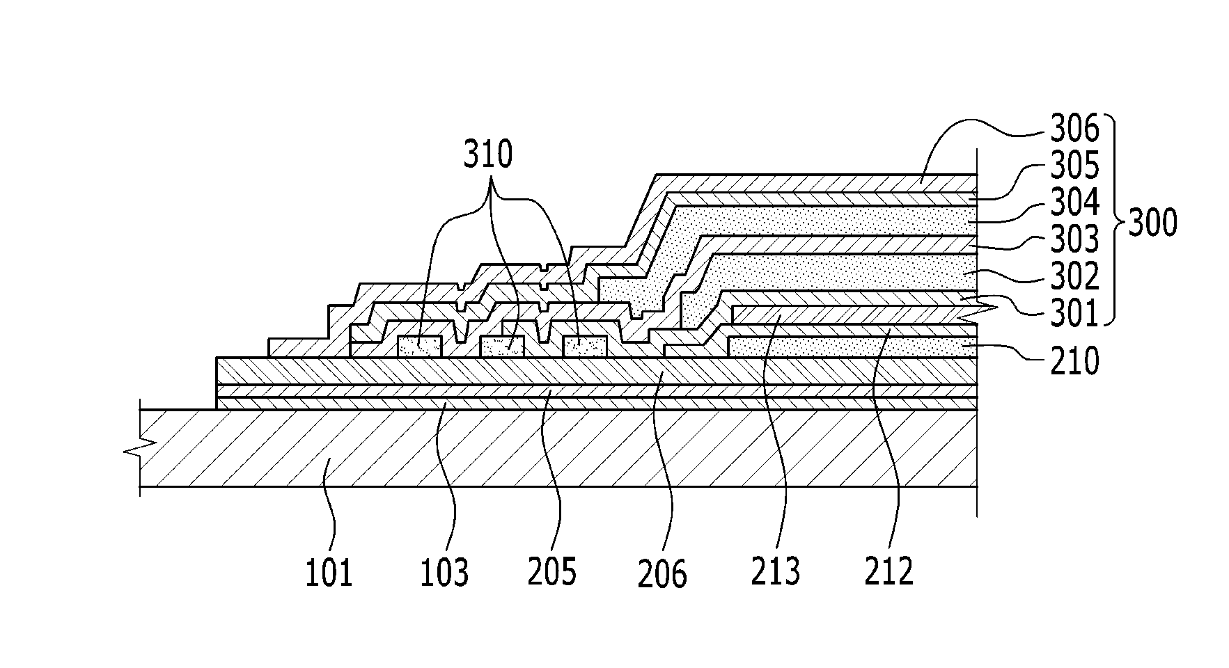
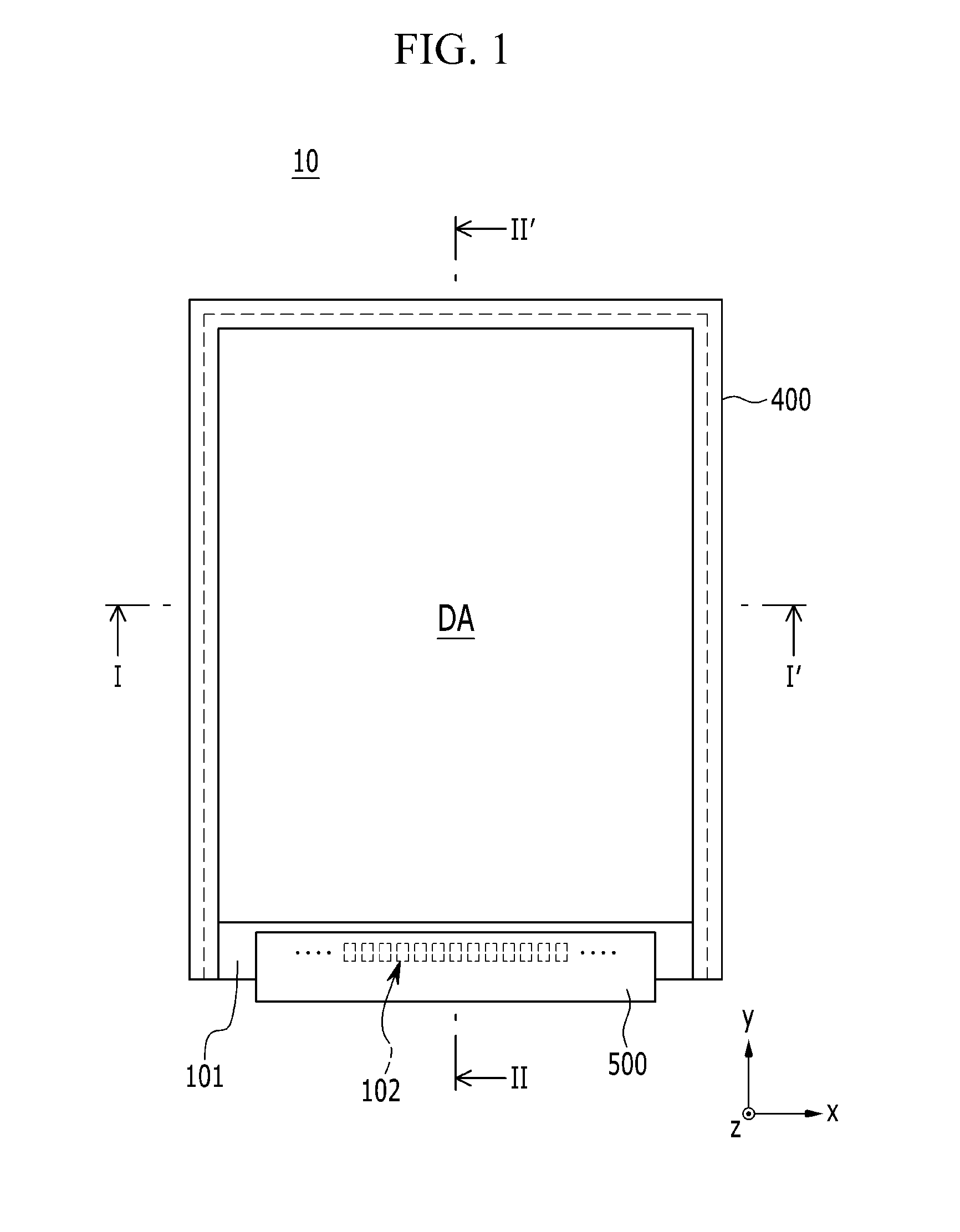
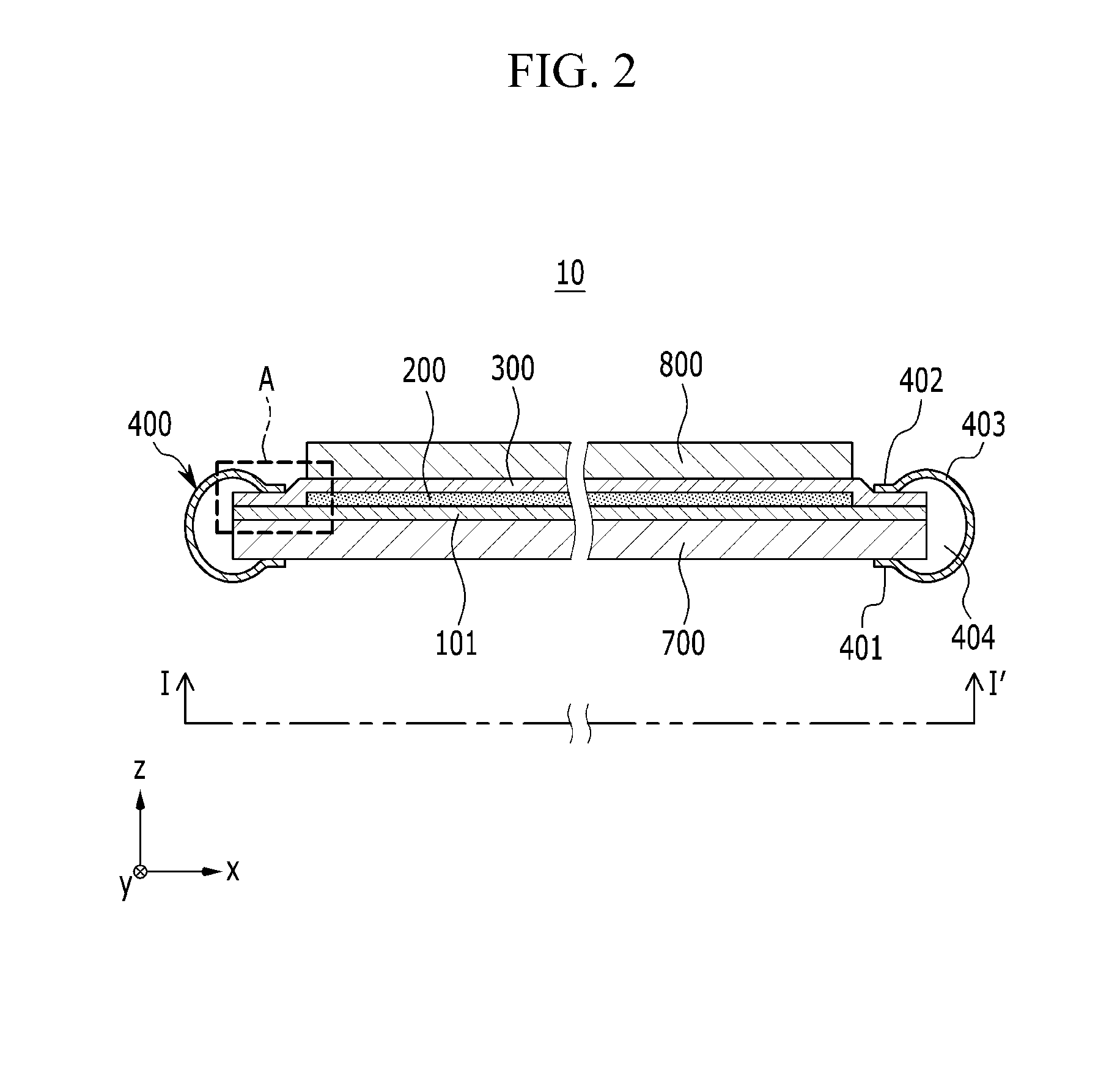
[0026]The present disclosure will be described more fully hereinafter with reference to the accompanying drawings, in which exemplary embodiments of the disclosure are shown. As those skilled in the art would realize, the described embodiments may be modified in various different ways, all without departing from the spirit or scope of the present disclosure.

[0027]It will be understood that when an element such as a layer, film, region, or substrate is referred to as being “on” another element, it can be directly on the other element or intervening elements may also be present. Further, in the specification, the word “on” means positioning on or below the object portion, but does not essentially mean positioning on the upper side of the object portion based on a gravity direction.

[0028]In addition, unless explicitly described to the contrary, the word “comprise” and variations such as “comprises” or “comprising”, will be understood to imply the inclusion of stated elements but not th...


PUM


Abstract

Provided is an organic light emitting diode display including a substrate; a display unit formed on the substrate and including a thin film transistor and an organic light emitting diode; a thin film encapsulation covering and encapsulating the display unit and formed by a laminated structure made of at least one first inorganic layer, a first organic layer, and a second inorganic layer; and a protective bezel fixed to the substrate and spaced apart from the side of the substrate to surround edges of the substrate and the thin film encapsulation.

Description

CLAIM OF PRIORITY[0001]This application claims the priority to and all the benefits accruing under 35 U.S.C. §119 of Korean Patent Application No. 10-2015-0027324 filed in the Korean Intellectual Property Office (KIPO) on Feb. 26, 2015, the entire contents of which are incorporated herein by reference.BACKGROUND OF THE INVENTION[0002]1. Field of Disclosure[0003]The described technology relates generally to an organic light emitting diode display, and more particularly, to an organic light emitting diode display including a thin film encapsulation.[0004]2. Description of the Related Art[0005]An organic light emitting diode display includes an organic light emitting diode including an anode (a hole injection electrode), an organic emission layer, and a cathode (an electron injection electrode). An electron and a hole are coupled with each other in the organic emission layer to generate an exciton, and light is emitted by energy generated when the exciton falls from an excited state to...

Claims


Application Information

Patent Timeline
Patent Type & Authority Applications(United States)
IPC IPC(8): H01L51/52
CPCH01L51/5237H01L51/5246H01L51/5253H10K50/8445H10K59/87H10K50/84H10K50/8426
Inventor JEONG, CHANG YONGKIM, MU GYEOMKIM, YONG IL
Owner SAMSUNG DISPLAY CO LTD
Why Eureka
Try Eureka