Reference voltage circuit
- Summary
- Abstract
- Description
- Claims
- Application Information
AI Technical Summary
Benefits of technology
Problems solved by technology
Method used
Image

Examples
Embodiment Construction
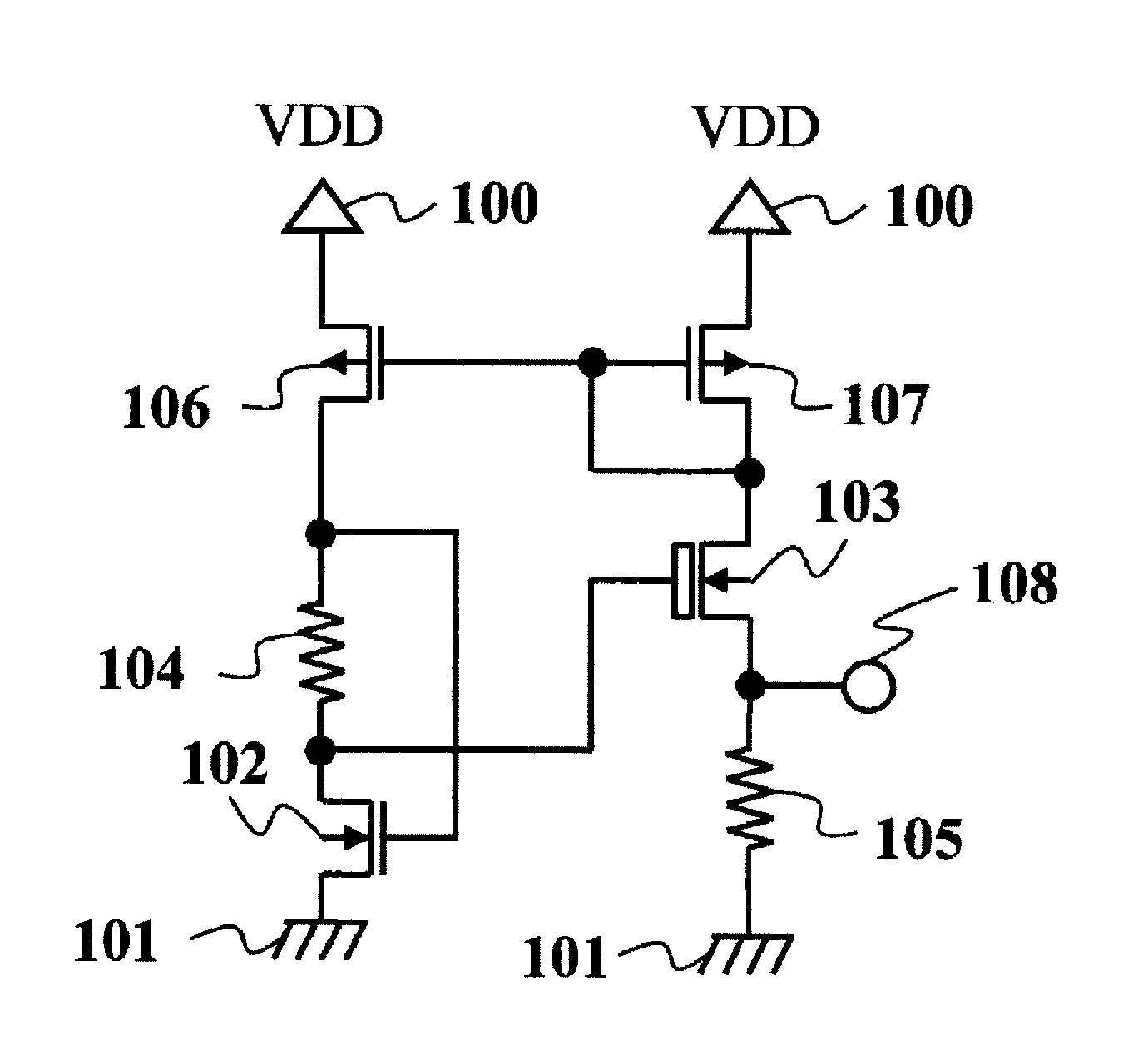
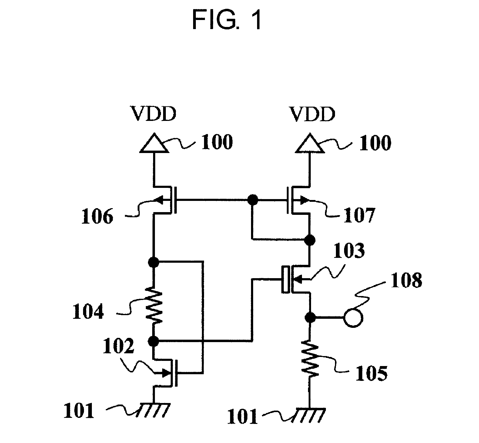
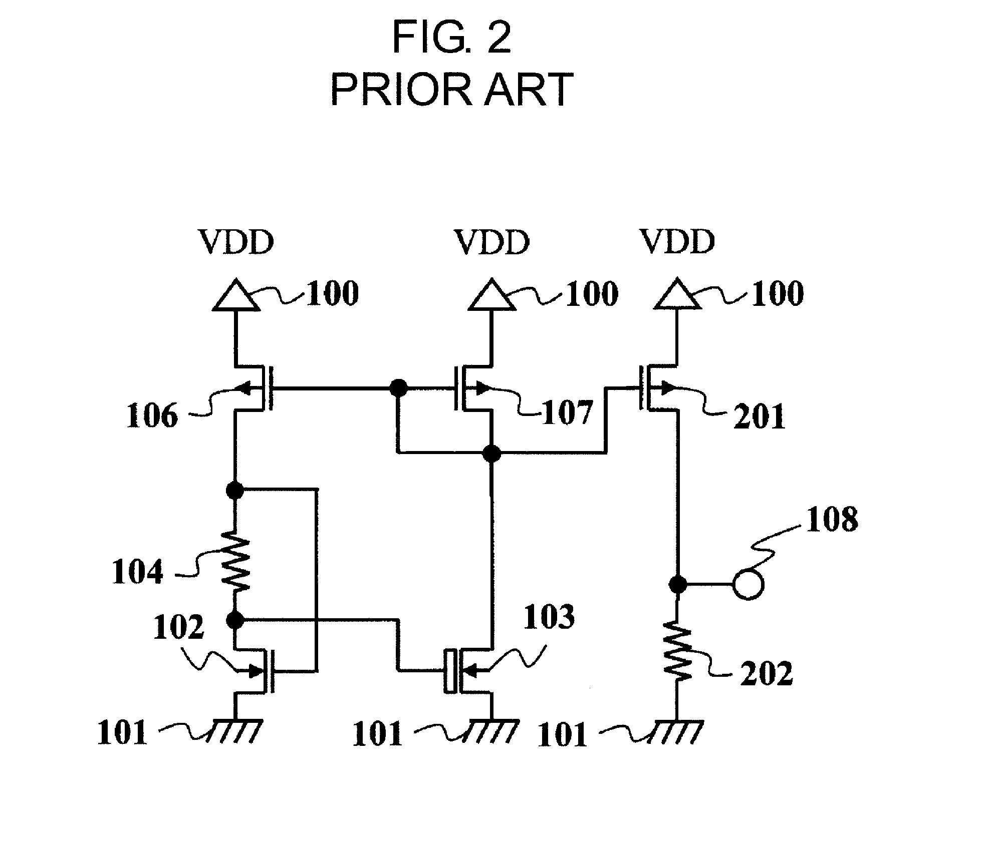
[0015]FIG. 1 is a circuit diagram for illustrating a reference voltage circuit according to an embodiment of the present invention. The reference voltage circuit according to this embodiment includes an NMOS transistor 102, an NMOS transistor 103, a PMOS transistor 106, a PMOS transistor 107, a resistor 104, a resistor 105, and an output terminal 108.
[0016]The NMOS transistor 102 has a gate and a drain connected to each other via the resistor 104, the drain being further connected to a gate of the NMOS transistor 103, the gate being further connected to a drain of the PMOS transistor 106. The NMOS transistor 103 has a drain connected to a drain and a gate of the PMOS transistor 107 and to a gate of the PMOS transistor 106, and a source connected to the GND terminal 101 via the resistor 105. The PMOS transistor 106 has a source connected to a power supply terminal 100. The source of the NMOS transistor 103 is further connected to the output terminal 108 of the reference voltage circu...
PUM
 Abstract
Description
Claims
Application Information
 - R&D
- Intellectual Property
- Life Sciences
- Materials
- Tech Scout
- Unparalleled Data Quality
- Higher Quality Content
- 60% Fewer Hallucinations
Browse by: Latest US Patents, China's latest patents, Technical Efficacy Thesaurus, Application Domain, Technology Topic, Popular Technical Reports.
© 2025 PatSnap. All rights reserved.Legal|Privacy policy|Modern Slavery Act Transparency Statement|Sitemap|About US| Contact US: help@patsnap.com