Image sensor and method of manufacturing the same

a technology of image sensor and manufacturing method, which is applied in the direction of diodes, semiconductor/solid-state device details, radio-controlled devices, etc., can solve problems such as difficult to getter, and achieve the effects of suppressing charge emission, reducing noise, and improving the gettering

Active Publication Date: 2016-09-29
CANON KK
View PDF6 Cites 10 Cited by
  • Summary
  • Abstract
  • Description
  • Claims
  • Application Information

AI Technical Summary

Benefits of technology

[0006]Some embodiments of the present invention provide a technique of reducing noise by...

Problems solved by technology

It is therefore difficult to getter, by this low-temperature annealing, an impurity such as a heavy metal in the defective...

Method used


Image

  • Image sensor and method of manufacturing the same
  • Image sensor and method of manufacturing the same
  • Image sensor and method of manufacturing the same

Examples


Embodiment Construction

[0017]A practical embodiment of an image sensor of the present invention will be described below with reference to the accompanying drawings. Note that in a description and the drawings below, common reference numerals denote common arrangements throughout the plurality of drawings. Therefore, the common arrangements will be described with reference to the plurality of drawings mutually and descriptions of the arrangements denoted by the common reference numerals will be omitted as needed.

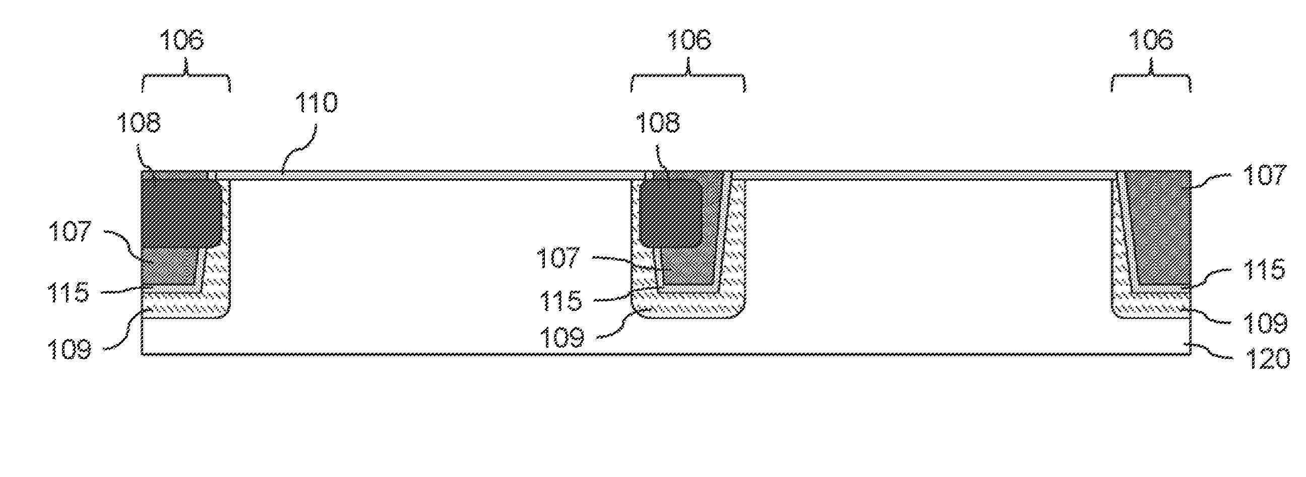
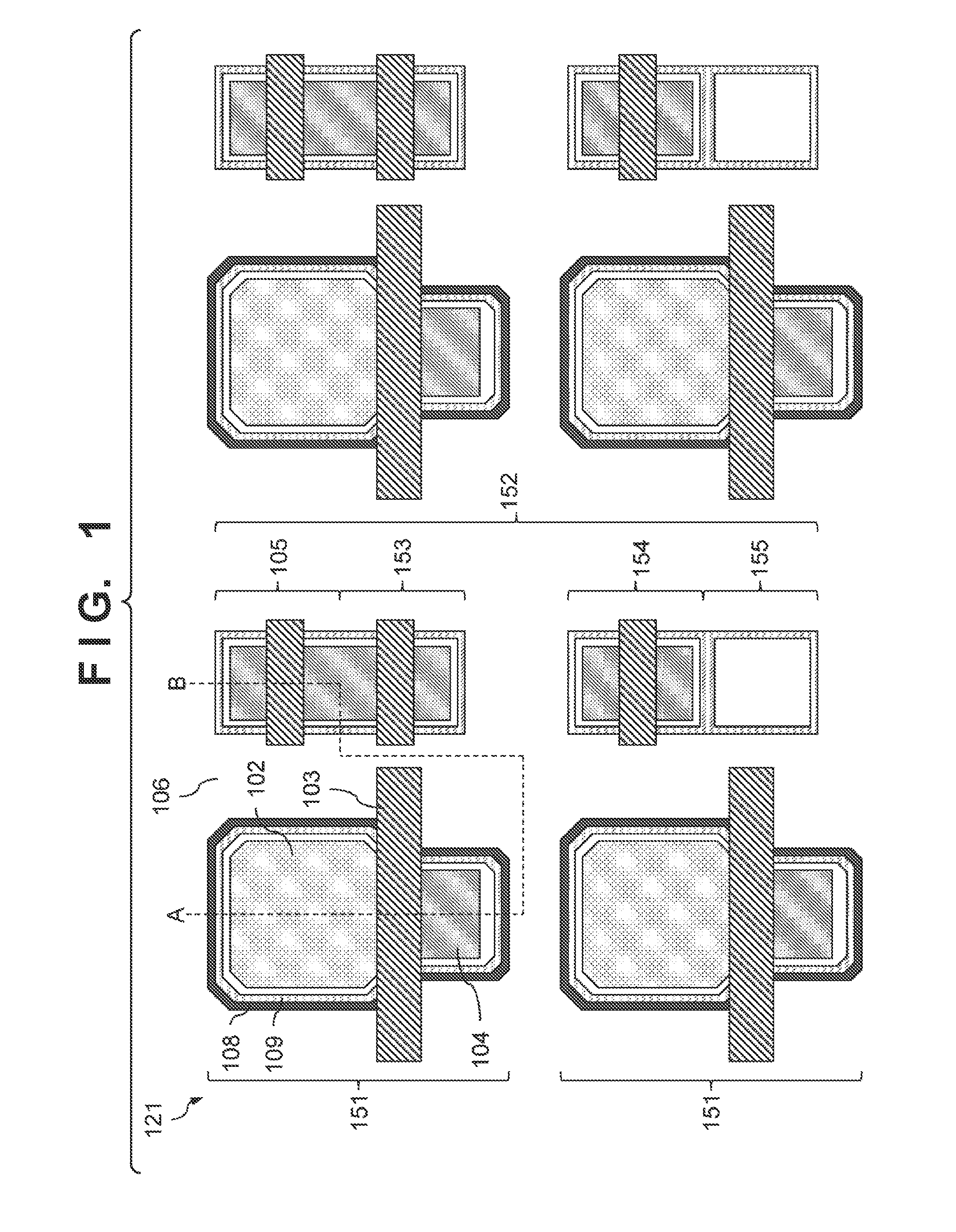
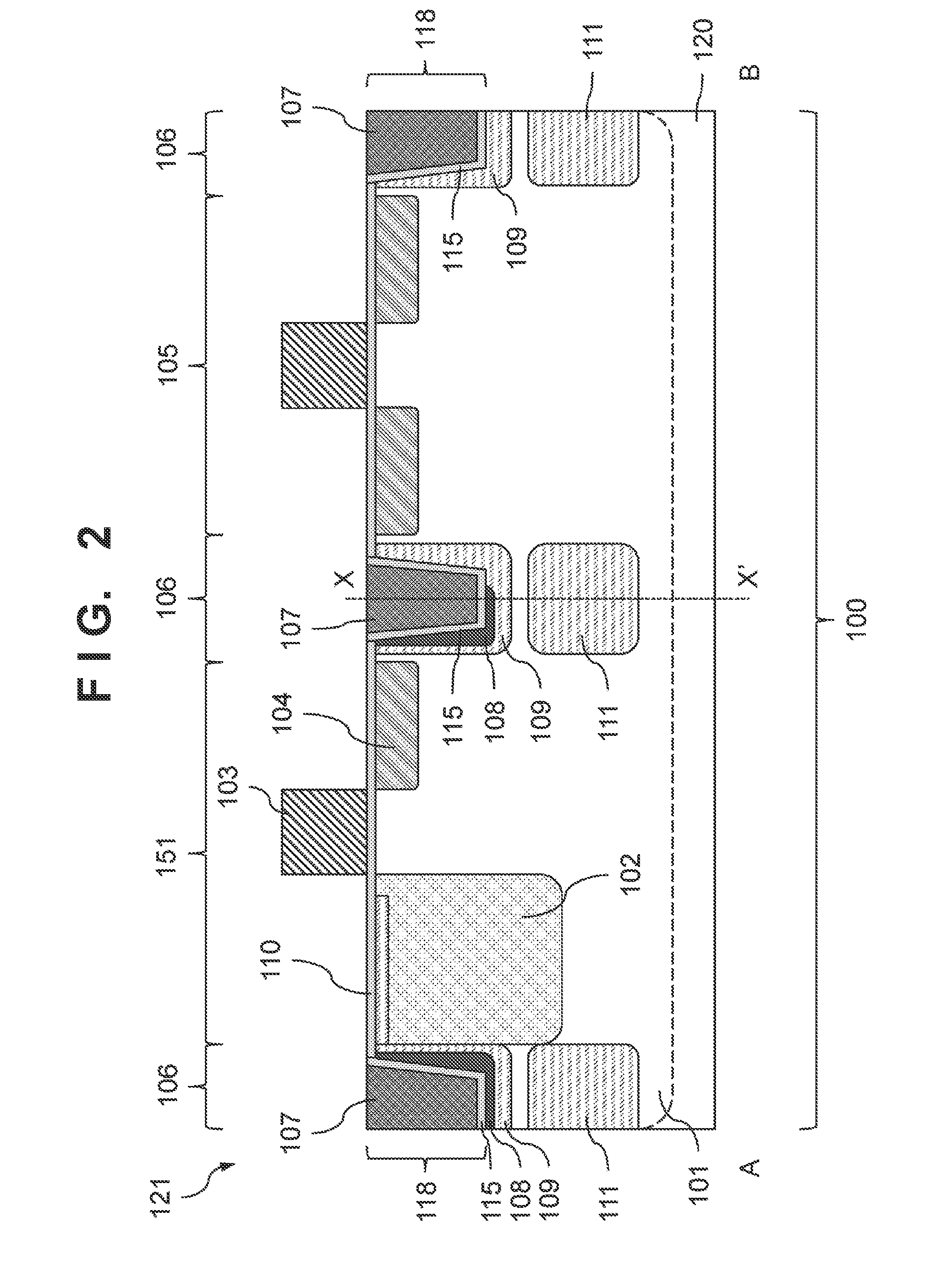
[0018]FIG. 1 is a plan view showing a pixel region of an image sensor 121 according to this embodiment. In FIG. 1, constituent elements such as a contact, a wiring layer, a color filter, a microlens, and a peripheral circuit region of the image sensor 121 are omitted for simplicity. The pixel region of the image sensor 121 includes first element regions 151 and a second element region 152. Those element regions are also referred to as active regions. Each first element region 151 includes a charge ...


PUM


Abstract

An image sensor is provided. The sensor comprises a plurality of photoelectric conversion elements each including a charge accumulation region of a first conductivity type arranged in a semiconductor substrate and an element isolation region arranged between the charge accumulation regions adjacent to each other. The element isolation region includes an insulator isolation portion arranged on an inner side of a trench on a surface of the semiconductor substrate, and includes a semiconductor region of a second conductivity type opposite to the first conductivity type arranged along a side surface of the insulator isolation portion. A gettering region is arranged between the semiconductor region and the insulator isolation portion along at least a part of the side surface of the insulator isolation portion.

Description

BACKGROUND OF THE INVENTION[0001]1. Field of the Invention[0002]The present invention relates to an image sensor and a method of manufacturing the same.[0003]2. Description of the Related Art[0004]A white spot is given as a drawback unique to an image sensor. The white spot is noise generated when an impurity such as a heavy metal or a crystal defect exists in a photoelectric conversion element. A defective layer is formed in a semiconductor substrate with respect to this noise and the impurity is gettered in the defective layer by annealing during a manufacturing process, reducing noise. In recent years, a technique of forming a defective layer in an element isolation region in the vicinity of a photoelectric conversion element has been proposed. Japanese Patent Laid-Open No. 2009-194269 has disclosed a structure which includes a defective layer in a position deeper than the bottom of a trench element isolation (STI) arranged above an element isolation region out of element isolati...

Claims


Application Information

Patent Timeline
IPC IPC(8): H01L27/146H01L23/26
CPCH01L27/14643H01L27/14603H01L27/1463H01L27/14698H01L27/14612H01L27/14689H01L23/26
Inventor KANEDA, TASUKU
Owner CANON KK
Why Eureka
Try Eureka