
Method and device for auto-calibration of multi-gate circuits

a multi-gate circuit and auto-calibration technology, applied in logic circuits, pulse generation by logic circuits, power consumption reduction, etc., can solve the problems of inability to meet the requirements of the final circuit, the introduction of mismatches of transistors, and the constraint of the fabrication method for integrated circuits

Active Publication Date: 2016-10-13
UNIV DE NICE +1
View PDF6 Cites 5 Cited by
  • Summary
  • Abstract
  • Description
  • Claims
  • Application Information

AI Technical Summary

Benefits of technology

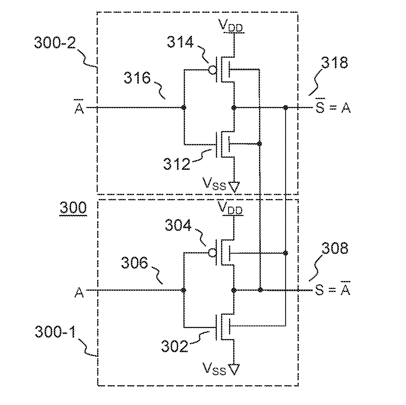
The present invention proposes a complementary-logic circuit that includes two logic cells composed of back-gate transistors. The first cell has one input and one output for delivering a first output signal. The second cell has the same number of inputs as the first cell and each input can receive a complementary signal to the input of the first cell. The second cell has one output for delivering a second output signal that is complementary to the first output signal of the first cell. The circuit is characterized in that the first output signal is applied to the back gate of each transistor in the second cell, and the second output signal is applied to the back gate of each transistor in the first cell. The technical effect of this invention is to provide a more efficient and effective logic circuit that can perform complex operations with high precision.

Problems solved by technology

However, the variability of the fabrication methods remains constraining for integrated circuits and it introduces mismatches of the transistors.
This difference in characteristics may introduce malfunctions of the final circuit, which may then no longer satisfy, for certain applications, the specifications demanded.
However, the known approaches for the implementation of calibration lead to an increase in the surface area of the final circuit through extra electronics, therefore to an increase in consumption and to an increase in overall cost.
Hence a problem to be solved is that of proposing a calibration solution for circuits which does not increase the surface area of the circuit, and which exhibits an immunity to the variability of the methods.
However, no known simple solution to this problem exists in FDSOI technology.

Method used


Image

  • Method and device for auto-calibration of multi-gate circuits
  • Method and device for auto-calibration of multi-gate circuits
  • Method and device for auto-calibration of multi-gate circuits

Examples


Embodiment Construction

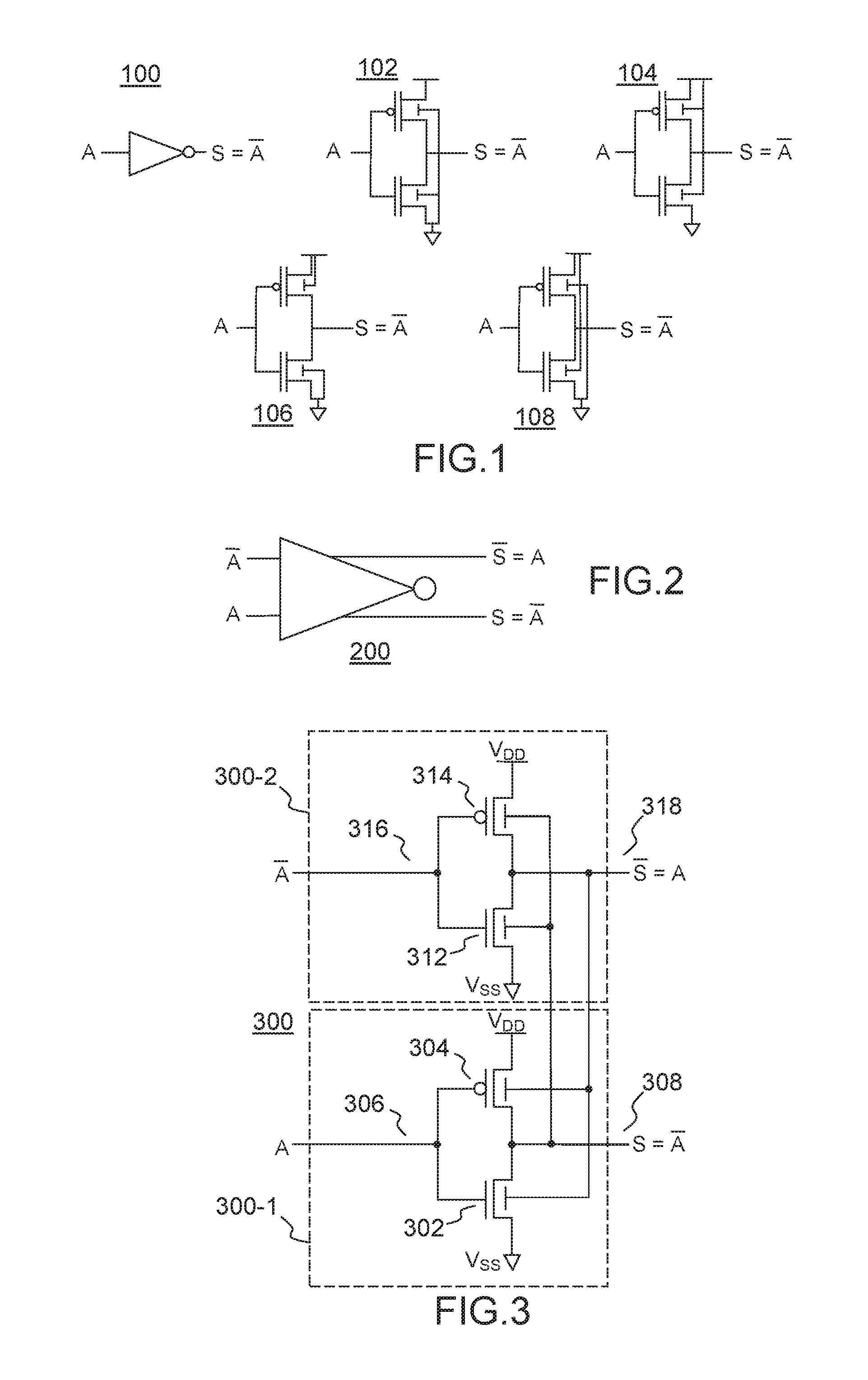
[0021]Reference is made to FIG. 1 where a logic conventional representation 100 of an inverter circuit having an input ‘I=A’ and delivering a complementary output ‘S=Ā’ is shown. A few examples of implementations of such an inverter in a back-gate transistors technology such as FDSOI CMOS technology are illustrated, where the back gates of the transistors can be connected to like voltages (102, 104) or to different voltages (106, 108). However, these examples are nonlimiting and the principles of the invention can apply to other technologies proposing dissymmetric transistors having asymmetric gates.

[0022]FIG. 2 illustrates, on a representation of an inverter circuit, the general principle of the invention which is to symmetrize the operation of the circuit according to complementary logic. The inverter circuit 200 of the invention comprises a complementary input and a complementary output. The input of the circuit receives a first signal ‘A’ and a second signal ‘Ā’ complementary to...


PUM


Abstract

A differential-logic logic circuit chained with another differential-logic circuit comprises a first logic cell composed of back-gate transistors, the first cell having a first input for receiving a first input signal and having an output for delivering a first output signal, and a second logic cell complementary to the first cell, composed of back-gate transistors, the second cell having as many inputs as the first cell, each input able to receive an input signal complementary to the respective input signal of the first cell, the second cell having an output for delivering a second output signal complementary to the first output signal of the first cell. The first output signal of the first cell is applied to the back gate of each transistor of the second cell, and the second output signal of the second cell is applied to the back gate of each transistor of the first cell.

Description

FIELD OF THE INVENTION[0001]The invention lies in the field of integrated circuits, and in particular that of multi-gate circuits of FinFET or FDSOI type.PRIOR ART[0002]Every year, new microelectronic technologies are available, affording innovations and improvements to our daily life. All this is possible by virtue of circuits of ever higher performance and ever more complex functions. This increase in performance has been made possible through the miniaturization of elementary components, namely transistors. Current technologies make it possible to design microchips having transistors with atomic dimensions. As the size of the transistors is reduced towards some ten nanometres, the variation of the dopants in the region of the channel directly causes a variation of the threshold voltage VTH between two transistors assumed to be identical and adjacent on one and the same microchip. Novel structures of MOSFET transistors have recently been proposed so as to reduce the variability of...

Claims


Application Information

Patent Timeline
IPC IPC(8): H03B27/00H03K19/0944H03K3/03H01L29/78
CPCH03B27/00H01L29/785H03K3/0322H01L29/7831H03K19/0944H03K19/0013H03K19/0027H03K19/01707H03K19/0948H03K17/16
Inventor JACQUEMOD, GILLES FERNANDDE FOUCAULD, EMERICFONSECA, ALEXANDRE BENJAMINLEDUC, YVESLORENZINI, PHILIPPE BERNARD PIERRE
Owner UNIV DE NICE
Learn More