A liquid crystal display device and a liquid crystal display panel thereof

a liquid crystal display and display panel technology, applied in non-linear optics, instruments, optics, etc., can solve the problems of failure to charge sharing, increase cost, decrease yield, etc., and achieve easy and effective detection and increase yield

Inactive Publication Date: 2016-10-20
TCL CHINA STAR OPTOELECTRONICS TECH CO LTD
View PDF0 Cites 1 Cited by
  • Summary
  • Abstract
  • Description
  • Claims
  • Application Information

AI Technical Summary

Benefits of technology

[0020]Comparing to the conventional technique, the sub pixel of the present LCD device and the present LCD panel is set on the insulating layer and next to the share sheet. The share sheet is electrically connected with the third TFT through a via and extends forward an end of the adjacent sub pixel. A share capacitance is set between the share sheet and the bottom common electrode of the adjacent sub pixel. A drain of the third TFT is coupled to the share capacitance so the two adjacent pixel units display solid color picture when short occurs between the adjacent sub pixel and the share capacitance. The detection is easy and effective so the yield is increased.

Problems solved by technology

It causes fail of the charge sharing.
This detection cannot investigate the short resulted from the connection of the ITO layer 2 and the sub pixel electrode 7 so the yield is decreased and the cost is increased.

Method used


Image

  • A liquid crystal display device and a liquid crystal display panel thereof
  • A liquid crystal display device and a liquid crystal display panel thereof
  • A liquid crystal display device and a liquid crystal display panel thereof

Examples


Embodiment Construction

[0030]To better and concisely explain the disclosure, the same name or the same reference number given or appeared in different paragraphs or figures along the specification should has the same or equivalent meanings while it is once defined anywhere of the disclosure.

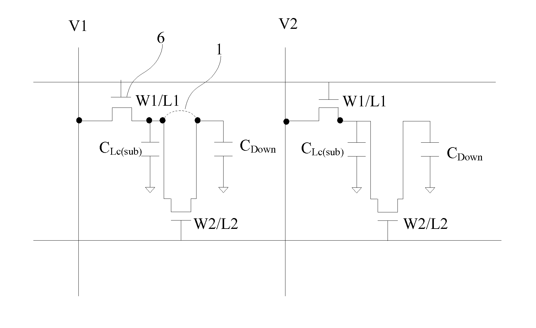
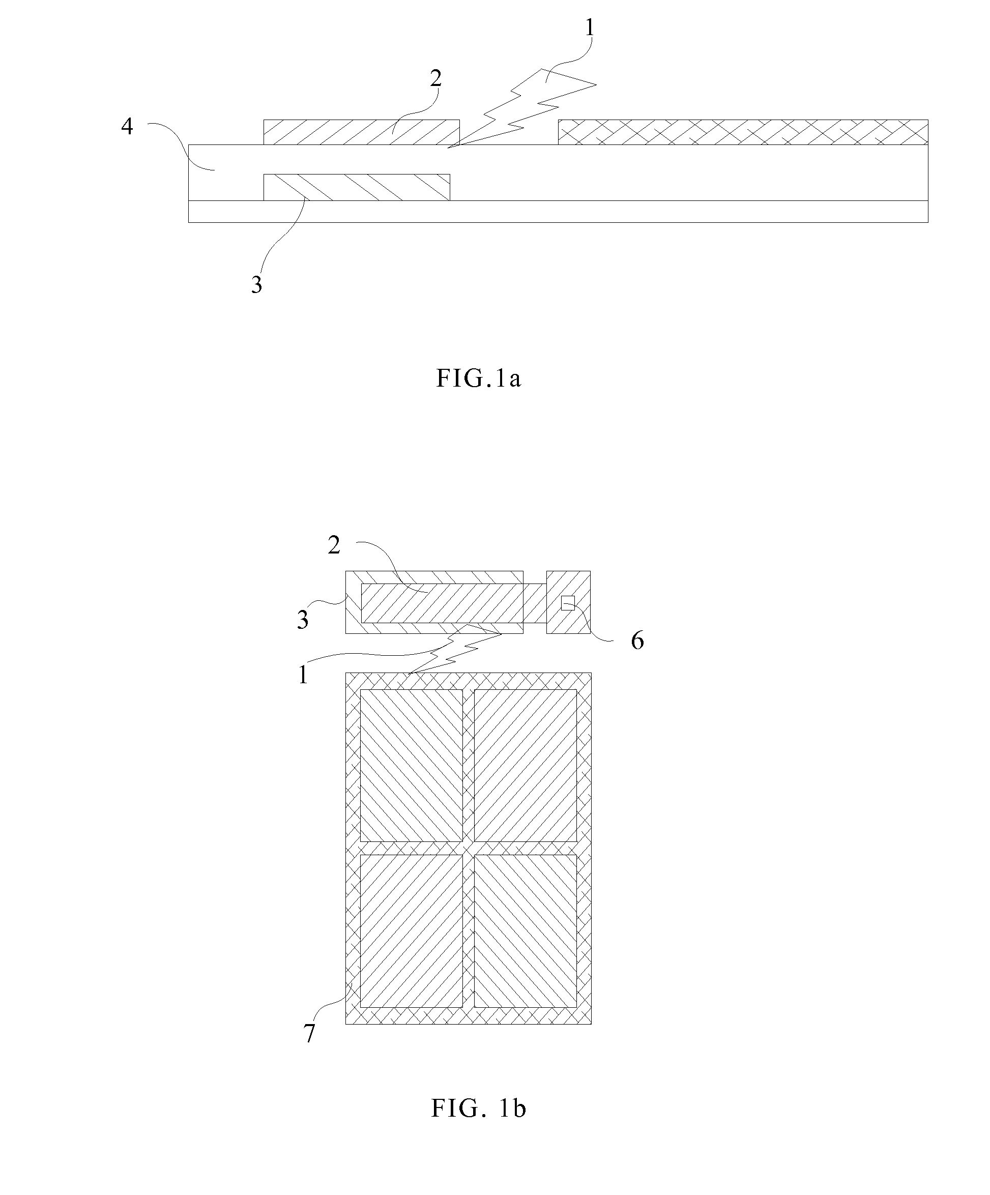
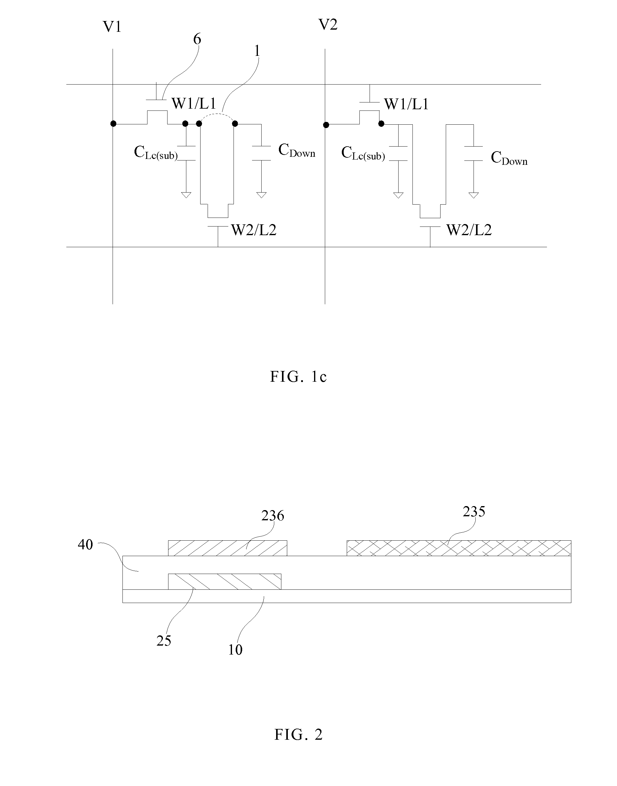
[0031]Referring FIGS. 2-5 together, FIG. 2 is a schematic view of a partial structure of a liquid crystal display (LCD) panel in accordance with an embodiment of the present invention, FIG. 3 is a top view of the LCD panel of FIG. 2, FIG. 4 is an equivalent circuit diagram of a pixel unit of the LCD panel, and FIG. 5 is an equivalent circuit diagram of two adjacent sub pixels of the LCD panel.

[0032]The LCD panel includes a top substrate (not shown here), a bottom substrate 10, and a liquid crystal (LC) layer (not shown here). The LC layer is set between the top substrate and the bottom substrate 10.

[0033]Referring FIG. 4, there is a top common electrode (not shown here) set on the top substrate. The bottom substrate 10...


PUM

PropertyMeasurementUnit
capacitanceaaaaaaaaaa
color shiftaaaaaaaaaa
chargeaaaaaaaaaa

Abstract

The present invention provides a liquid crystal display (LCD) panel including a top substrate, a bottom substrate, and a liquid crystal (LC) layer. The bottom substrate further includes an insulating layer between a bottom common electrode and a share sheet. A sub pixel is set on the insulating layer and next to the share sheet. The share sheet is electrically connected with A third thin film transistor (TFT) through a via and extends forward an end of the adjacent sub pixel. A share capacitance is set between the share sheet and the bottom common electrode of the adjacent sub pixel. A drain of the third TFT is coupled to the share capacitance so the two adjacent pixel units display solid color picture when short occurs between the adjacent sub pixel and the share capacitance. The detection is easy and effective so the yield is increased.

Description

BACKGROUND[0001]1. Technical Field[0002]The present invention relates to display field, and more particularly, to a liquid crystal display device and a liquid crystal display panel thereof.[0003]2. Description of the Related Art[0004]For correcting the color shift at the big viewing angle in the liquid crystal display (LCD) panel of vertical alignment (VA), it adopts pixel design of charge sharing. That is, the pixel has a main pixel and a sub pixel. In regular displaying mode, the charge gate opens and the sharing gate closes. The main pixel and the pixel electrode are charged to the same potential. Then, the charge gate closes and the share gate opens. The potential of the sub pixel is lower than that of the main pixel because of the share capacity (Cst3). The difference of the potential makes the orientations of the liquid crystal molecules different in two displaying regions so it corrects the color shift at the big viewing angle.[0005]The product can adopt the pixel structure s...

Claims


Application Information

Patent Timeline
Patent Type & Authority Applications(United States)
IPC IPC(8): G02F1/1362G02F1/1333G02F1/1343G02F1/1368
CPCG02F1/136286G02F1/1368G02F1/133345G02F2001/134354G02F1/13624G02F2201/121G02F2001/134345G02F1/134309G02F1/1343G02F1/136213G02F1/136227G02F1/136259G02F1/134345G02F1/134354
Inventor CHEN, CHENG-HUNGWANG, ZUI
Owner TCL CHINA STAR OPTOELECTRONICS TECH CO LTD
Why Eureka
Try Eureka