Back-Illuminated Sensor Chips

a sensor chip and backlighting technology, applied in the field of backlighting sensor chips, can solve the problems of difficult lens modification, increased chip stress, and non-uniform imaging characteristic of a central area, and achieve the effect of increasing the light sensibility of the peripheral portion and more uniform imaging quality of the camera

Active Publication Date: 2016-10-27
OMNIVISION TECH (SHANGHAI) CO LTD
View PDF10 Cites 0 Cited by
  • Summary
  • Abstract
  • Description
  • Claims
  • Application Information

AI Technical Summary

Benefits of technology

[0006]It is an objective of the present invention to provide a back-illuminated sensor chip which can solve the aforementioned problem of lens-caused non-uniform imaging quality arising from use of the conventional cameras.
[0015]A back-illuminated sensor chip according to the present invention includes a logic area and a pixel area. The pixel area includes a peripheral portion and a central portion surrounded by the peripheral portion. The peripheral and central portions together form a step-like configuration with the peripheral portion protruding outward beyond the central portion. Therefore, the peripheral portion of the pixel area is located nearer to a light source during imaging. As a result, in light incident on the back-illuminated sensor chip, a portion of the light received by the peripheral portion is greater than a portion received by the central portion, thereby resulting in increased light sensibility of the peripheral portion, which can offset lens-caused non-uniformity in imaging characteristics between central and peripheral areas of a camera in which the sensor chip is used, i.e., resulting in more uniform imaging quality of the camera.

Problems solved by technology

Focusing of a conventional camera lens is typically associated with the problem of non-uniformity in imaging characteristic between a central area and a peripheral area of the lens.
This phenomenon depends on the nature of the lens and is thus hard to be improved through lens modifications.
Although this is theoretically capable of solving the non-uniform imaging problem of the conventional devices, formation of the arc-shaped silicon substrate can introduce additional stress to the chip, which has the following two possible consequences: 1) cracking of the chip; and 2) a certain degree of deterioration of imaging quality, particularly in terms of, for example, dark current, white pixel and noise.
Avoidance of these risks may impose extremely strict requirements on the production process and thus lead to a significant reduction in the yield.

Method used


Image

  • Back-Illuminated Sensor Chips
  • Back-Illuminated Sensor Chips
  • Back-Illuminated Sensor Chips

Examples


embodiment 1

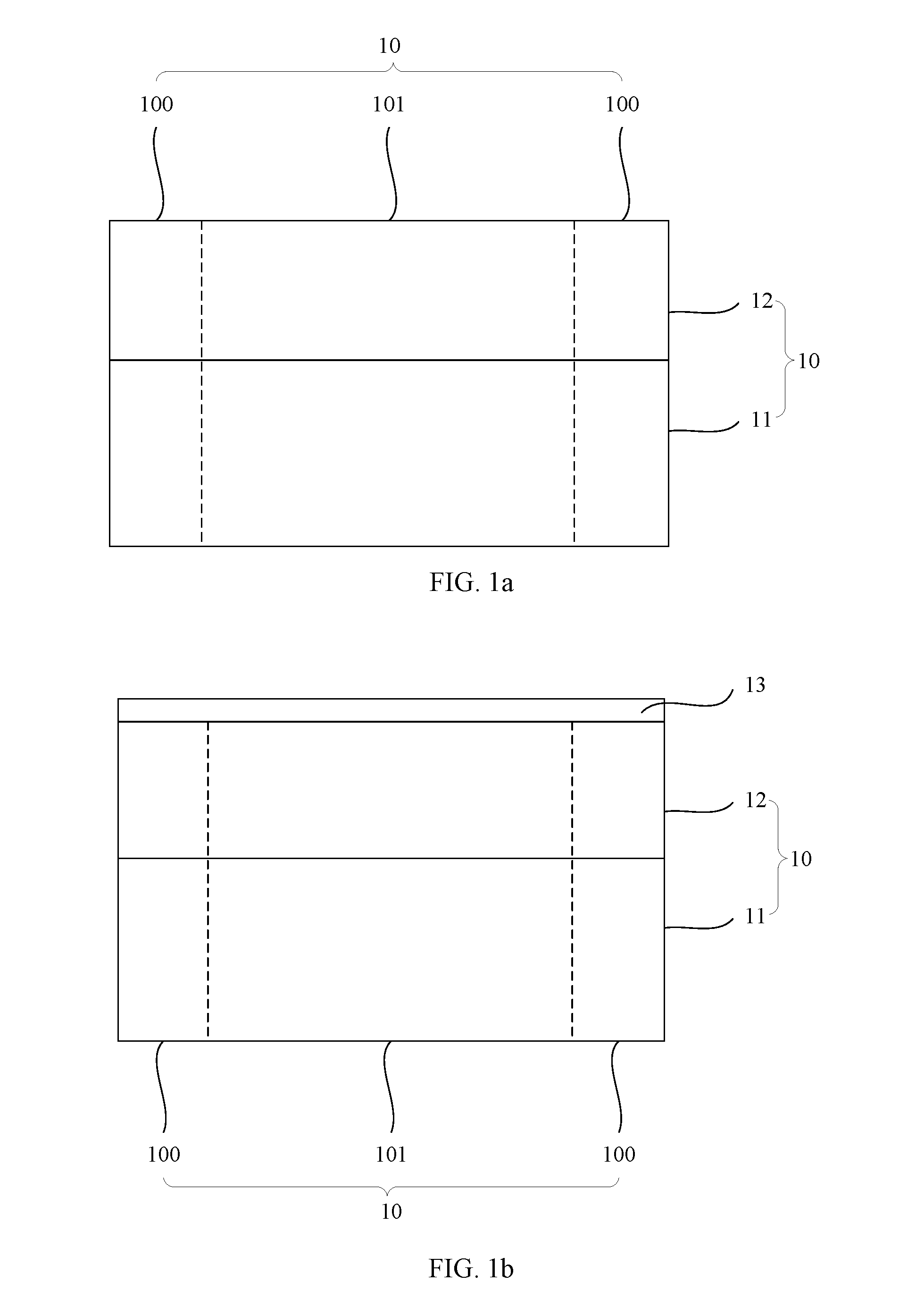
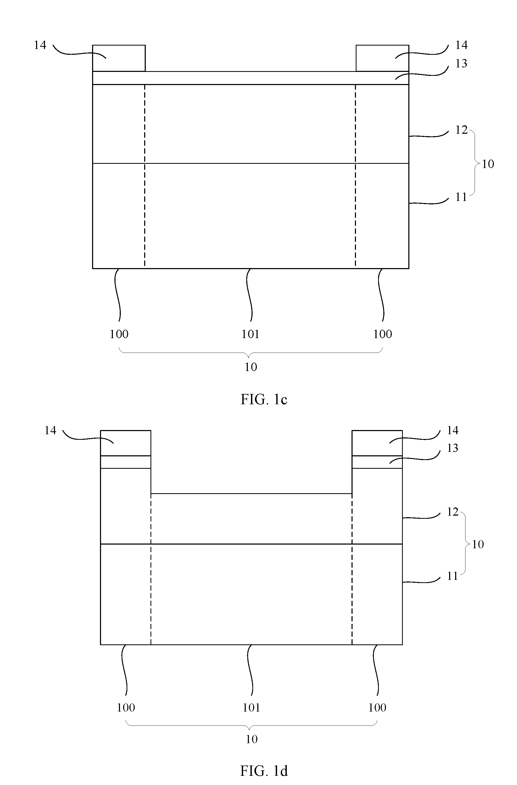
[0020]Referring to FIGS. 1a to 1e, which are cross-sectional views illustrating the formation of a pixel area in the construction of a back-illuminated sensor chip in a fabrication method of the back-illuminated sensor chip according to a first embodiment of the present invention.

[0021]At first, a composite substrate consisting of a device wafer and a carrier wafer (bonded together) is provided and the backside of the device wafer is thinned. The composite substrate includes a plurality of chip dies each having a pixel area and a logic area surrounding the pixel area. FIG. 1a shows a pixel area 10 of one of the chip dies, which includes a portion of the device wafer 12 and a portion of the carrier wafer 11. Further, as shown in FIG. 1a, the pixel area 10 includes a peripheral portion 100 and a central portion 101 surrounded by the peripheral portion 100. According to embodiments disclosed herein, the composite substrate may be silicon or silicon-germanium, and so forth. Preferably, ...

embodiment 2

[0031]This embodiment differs from Embodiment 1 in that a concentration of ions implanted in the peripheral portion 100 is higher than a concentration of ions implanted in the central portion 101. Here, reference may be made to FIG. 1e. Specifically, a back-illuminated sensor chip according to this embodiment includes a logic area (not shown) and a pixel area 10. The pixel area 10 includes a peripheral portion 100 and a central portion 101 surrounded by the peripheral portion 100. The peripheral portion 100 and central portion 101 together form a step-like configuration with the peripheral portion 100 protruding outward beyond the central portion 101. In addition, a concentration of ions implanted in the peripheral portion 100 is higher than a concentration of ions implanted in the central portion 101.

[0032]More specifically, according to embodiments disclosed herein, during the manufacture of the device wafer 12 (i.e., before the backside of the device wafer 12 is thinned), multipl...

embodiment 3

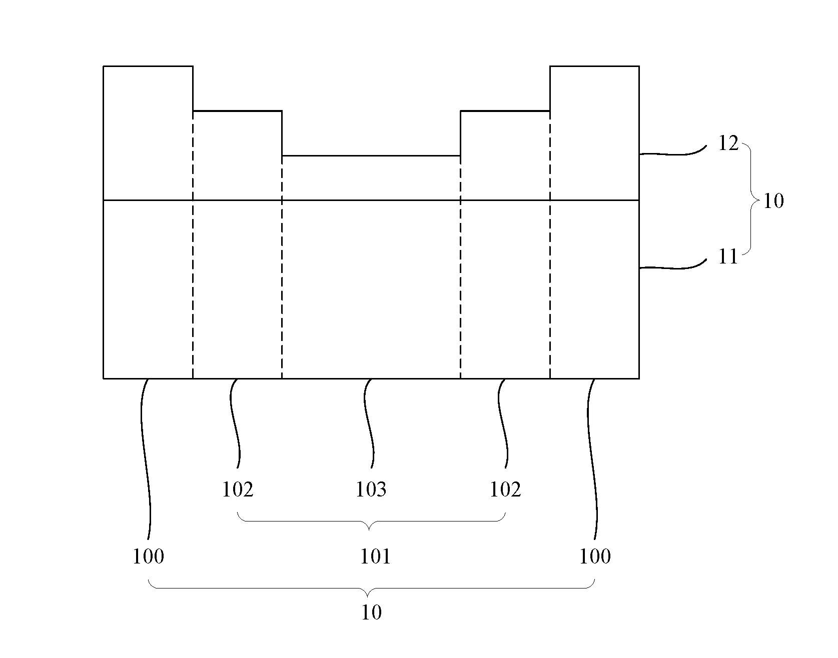
[0042]This embodiment differs from Embodiment 1 in that the central portion 101 of the pixel area 10 is further partitioned into a first portion 103 centrally situated in the central portion 101 and a second portion 102 surrounding the first portion 103. The second portion 102 and the first portion 103 together form a step-like configuration, in which the second portion 102 has a height greater than a height of the first portion 103. In other words, compared to Embodiment 1, the pixel area 10 according to this embodiment has a finer configuration which can fit better with a corresponding lens to form a camera with more uniform imaging characteristics.

[0043]This embodiment can be implemented by carrying out the steps illustrated in FIGS. 3a to 3d, in addition to those shown in FIGS. 1a to 1d (i.e., the step shown in FIG. 1e is not performed in this embodiment), which are also referenced in the description of Embodiment 1.

[0044]In other words, after the step shown in FIG. 1d has been ...


PUM


Abstract

A back-illuminated sensor chip is disclosed, which includes one or more pixel areas each including a plurality of pixels located in a plane and arranged in a matrix. Each pixel area includes: a central portion consisting of a plurality of first pixels located in vicinity of a center of the pixel area; and a peripheral portion surrounding the central portion and consisting of the other pixels in the pixel area than the first pixels. The plurality of first pixels have a first height in a vertical direction perpendicular to the plane, and the pixels in the peripheral portion have a second height in the vertical direction that is greater than the first height so that the peripheral portion protrudes outward beyond the central portion and is thus located nearer to a light source during imaging than the central portion. As a result, light sensibility of the peripheral portion is increased.

Description

CROSS-REFERENCES TO RELATED APPLICATIONS[0001]This application claims the priority of Chinese patent application number 201510197708.5, filed on Apr. 23, 2015, the entire contents of which are incorporated herein by reference.TECHNICAL FIELD[0002]The present invention relates to integrated circuit (IC) fabrication and, in particular, to back-illuminated sensor chips.BACKGROUND[0003]Cameras are one of the major applications of image sensors. A camera is essentially consisted of an image sensor and a proper lens. Focusing of a conventional camera lens is typically associated with the problem of non-uniformity in imaging characteristic between a central area and a peripheral area of the lens. As a result, an image captured by such a lens generally has a lower quality in its peripheral area than in its central area in terms of, e.g., clarity and brightness. This phenomenon depends on the nature of the lens and is thus hard to be improved through lens modifications.[0004]In order to solv...

Claims


Application Information

Patent Timeline
Patent Type & Authority Applications(United States)
IPC IPC(8): H01L27/146
CPCH01L27/1464H01L27/14643H01L27/1461H01L27/14605H01L27/14607H01L27/14687H01L27/14689
Inventor LIN, FENGLI, QUANBAOYE, GUO
Owner OMNIVISION TECH (SHANGHAI) CO LTD
Why Eureka
Try Eureka