Display device and multi display device using the same

a multi-display and display device technology, applied in the direction of casings/cabinets/drawers, casings/cabinets/drawers, instruments, etc., can solve the problems of cof or tcp damage, and achieve the effect of reducing or preventing a width increase of the non-display area

Active Publication Date: 2016-11-10
SAMSUNG DISPLAY CO LTD
View PDF3 Cites 6 Cited by
  • Summary
  • Abstract
  • Description
  • Claims
  • Application Information

AI Technical Summary

Benefits of technology

[0009]Exemplary embodiments of the present invention provide a display device which may minimize an area where a display panel and a top chassis overlap, may reduce or prevent damage in a chip on film (COF), or a tape carrier package (TCP) and may reduce or prevent damage to a multi-display device using the display device.
[0026]According to embodiments of the present invention, a part of the top chassis in contact with the flexible printed circuit board may be omitted, thereby preventing a flexible printed circuit board from being pressed and damaged by a top chassis.
[0027]In a multi-display device using the display device according to an embodiment of the present invention, the protrusion formed on a top chassis of one display device may be disposed in an opening in a top chassis of another display device, thereby reducing or preventing a width increase of the non-display area.

Problems solved by technology

In the multi-display device where a plurality of coupled display devices are used, the display panel and the top chassis may be adjacently disposed due to the weight of display devices that are adjacently disposed, and damage may occur in the COF or TCP.

Method used


Image

  • Display device and multi display device using the same
  • Display device and multi display device using the same
  • Display device and multi display device using the same

Examples


Embodiment Construction

[0038]Hereinafter, exemplary embodiments of the present invention will be described in more detail with reference to the accompanying drawings. The present invention may, however, be embodied in many different forms and should not be construed as being limited to the embodiments disclosed herein.

[0039]Throughout the specification, when an element is referred to as being “connected” to another element, the element may be “directly connected” to the other element, or “electrically connected” to the other element with one or more intervening elements interposed therebetween.

[0040]Like reference numerals may refer to like elements throughout the specification and drawings.

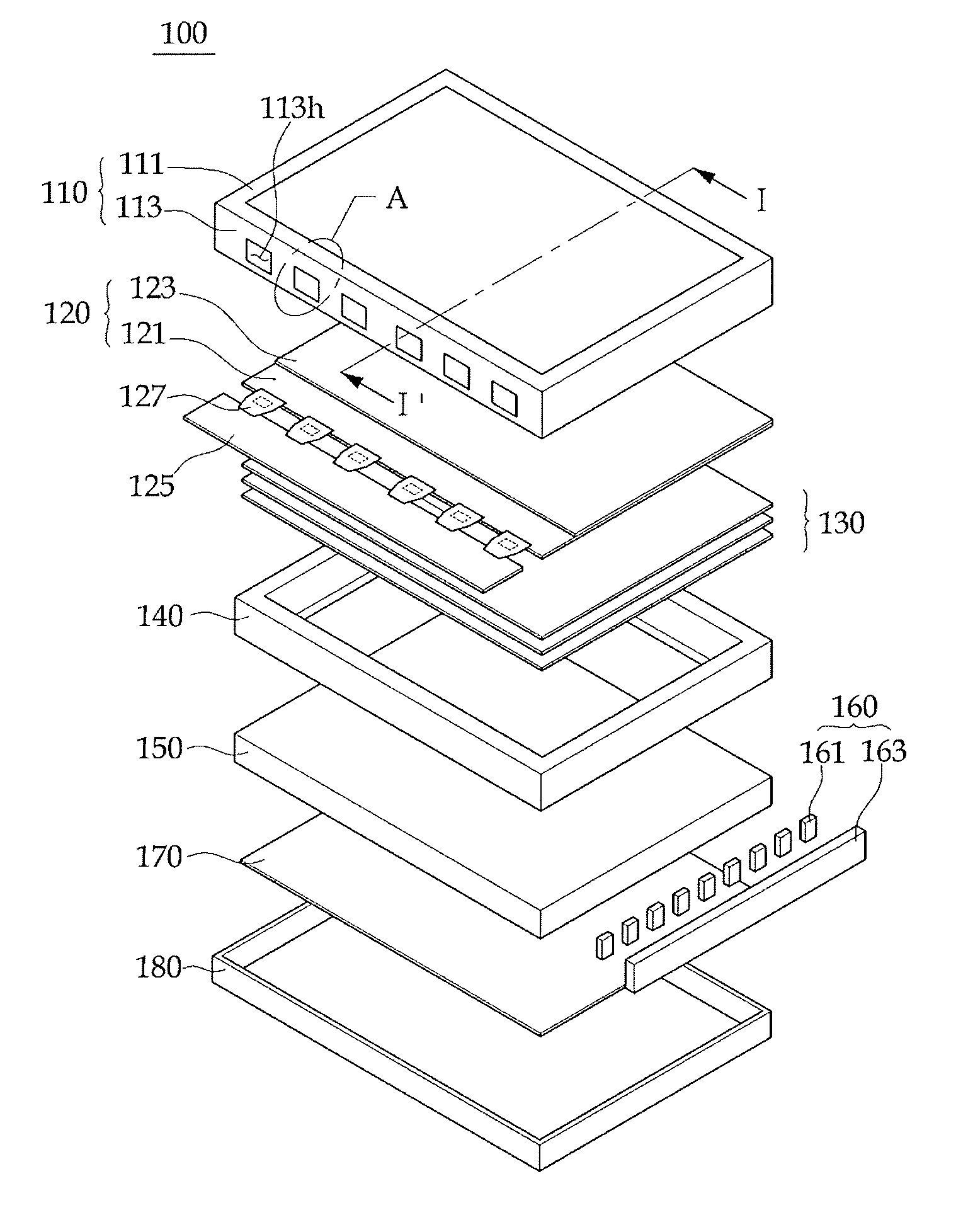
[0041]Hereinafter, a liquid crystal display (LCD) may be included in the display device according to an exemplary embodiment of the present invention. However, exemplary embodiments of the present invention can be applied to an organic light emitting diode (OLED) display or a plasma display panel (PDP).
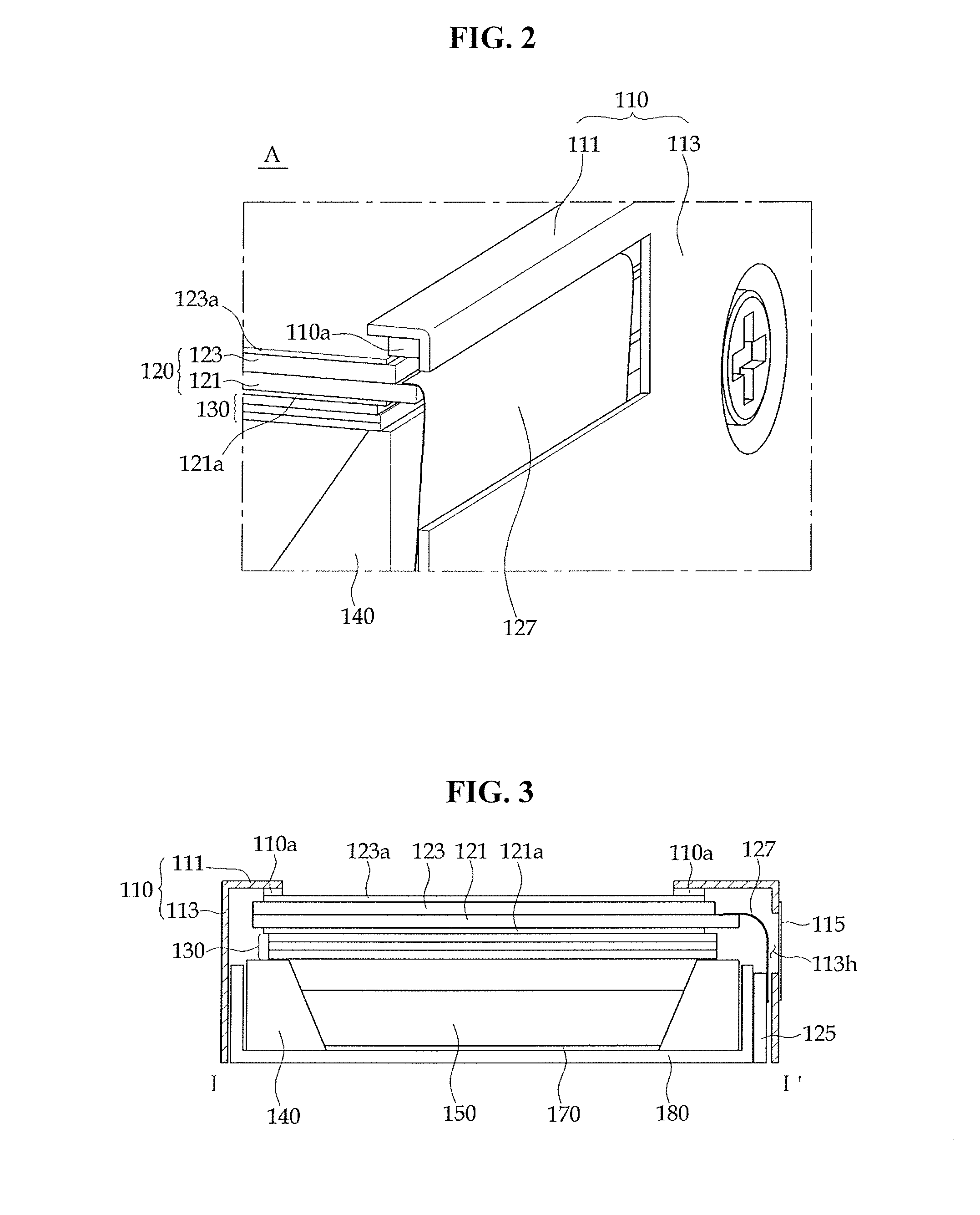
[0042]FIG. 1 is ...


PUM

PropertyMeasurementUnit
flexibleaaaaaaaaaa
areaaaaaaaaaaa
sizeaaaaaaaaaa

Abstract

A display device includes: a display panel; a bottom chassis in which the display panel is accommodated; a driving circuit substrate disposed on an outside surface of the bottom chassis; at least one flexible printed circuit board connecting the display panel to the driving circuit substrate; and a top chassis configured to cover an edge portion of a top surface and side surfaces of the display panel, wherein the top chassis has an opening formed in an area in contact with the flexible printed circuit board.

Description

CROSS-REFERENCE TO RELATED APPLICATION[0001]This application is a divisional of U.S. application Ser. No. 14 / 591,343, filed on Jan. 7, 2015, which claims priority under 35 U.S.C. §119 to Korean Patent Application No. 10-2014-0090274, filed on Jul. 17, 2014 in the Korean Intellectual Property Office, the disclosure of which is incorporated by reference herein in its entirety.1. TECHNICAL FIELD[0002]Exemplary embodiments of the present invention relate to a display device, and more particularly to a display device having multi-displays.2. DISCUSSION OF RELATED ART[0003]Examples of display devices may include a liquid crystal display (LCD), an organic light emitting diode (OLED) display, a plasma display panel (PDP), and an electrophoretic display (EPD).[0004]Display devices may include a display panel on which a plurality of pixels for displaying images are disposed, a driving printed circuit board (PCB) disposed on one side surface of the display panel, and a chip on film (COF), or a...

Claims


Application Information

Patent Timeline
Patent Type & Authority Applications(United States)
IPC IPC(8): G02F1/1333G02F1/1343H05K1/14G02F1/1368H05K5/00H05K5/02
CPCG02F1/133308H05K5/0021H05K5/0217H05K1/147G02F1/1368G02F1/134336G02F2001/13332H05K2201/10136G02F2201/123G02F1/133514G02F2201/121G02F1/13439G02F2001/133314H05K2201/10128G02F1/13452G02F1/133314G02F1/13332H05K7/02
Inventor YUN, SU YOUNGLEE, SUNG HUNPARK, JOO HYUK
Owner SAMSUNG DISPLAY CO LTD
Why Eureka
Try Eureka