
Pixel structure and pixel array having the same

a pixel array and structure technology, applied in non-linear optics, instruments, optics, etc., can solve problems such as unnatural side view images of display panels, blue-bias, green-bias or red-bias,

Active Publication Date: 2016-11-24
AU OPTRONICS CORP
View PDF2 Cites 11 Cited by
  • Summary
  • Abstract
  • Description
  • Claims
  • Application Information

AI Technical Summary

Benefits of technology

The invention is about a new pixel structure design that solves the problem of color shifting in side view images. The design adjusts the spacing of slits in the electrodes of the pixel structure. This results in different widths for the slits of each electrode, which helps to suppress yellow-bias and green-bias at certain gray levels, which can cause color shimming. Overall, the design improves the quality of images captured by the pixel structure.

Problems solved by technology

Limited by optical characteristics of the liquid crystal molecules, such type of the LCD panel may have a color shift phenomenon or inadequate color saturation under different viewing angles.
Although the aforementioned methods for resolving the color shift phenomenon or inadequate color saturation can mitigate a problem of white-bias (color washout) in case of a large viewing angle (side view), a side view image as compared to a front view image still has problems of blue-bias, green-bias or red-bias under different viewing angles.
Namely, a problem of color shift in a side view occurs, and this causes the side-view image of the display panel to look unnatural.

Method used


Image

  • Pixel structure and pixel array having the same
  • Pixel structure and pixel array having the same
  • Pixel structure and pixel array having the same

Examples


Embodiment Construction

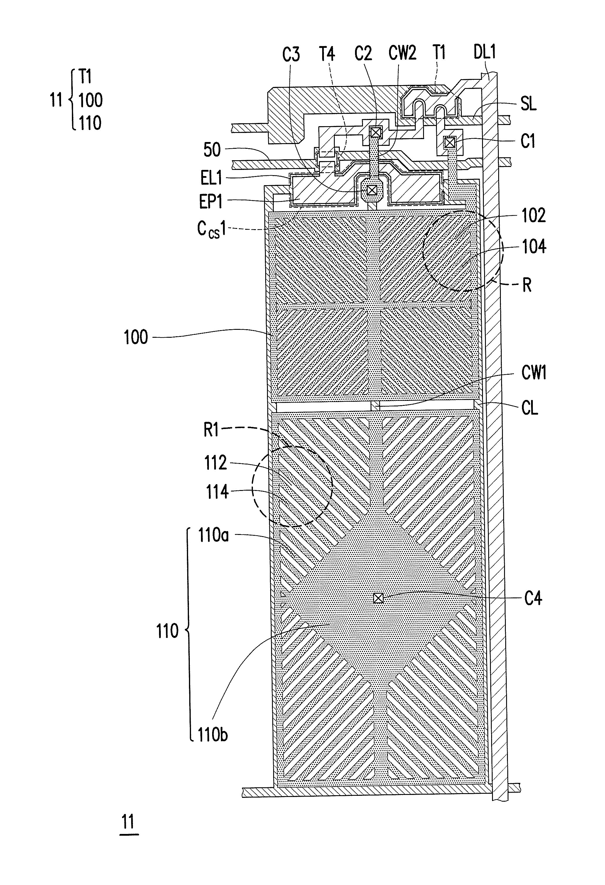
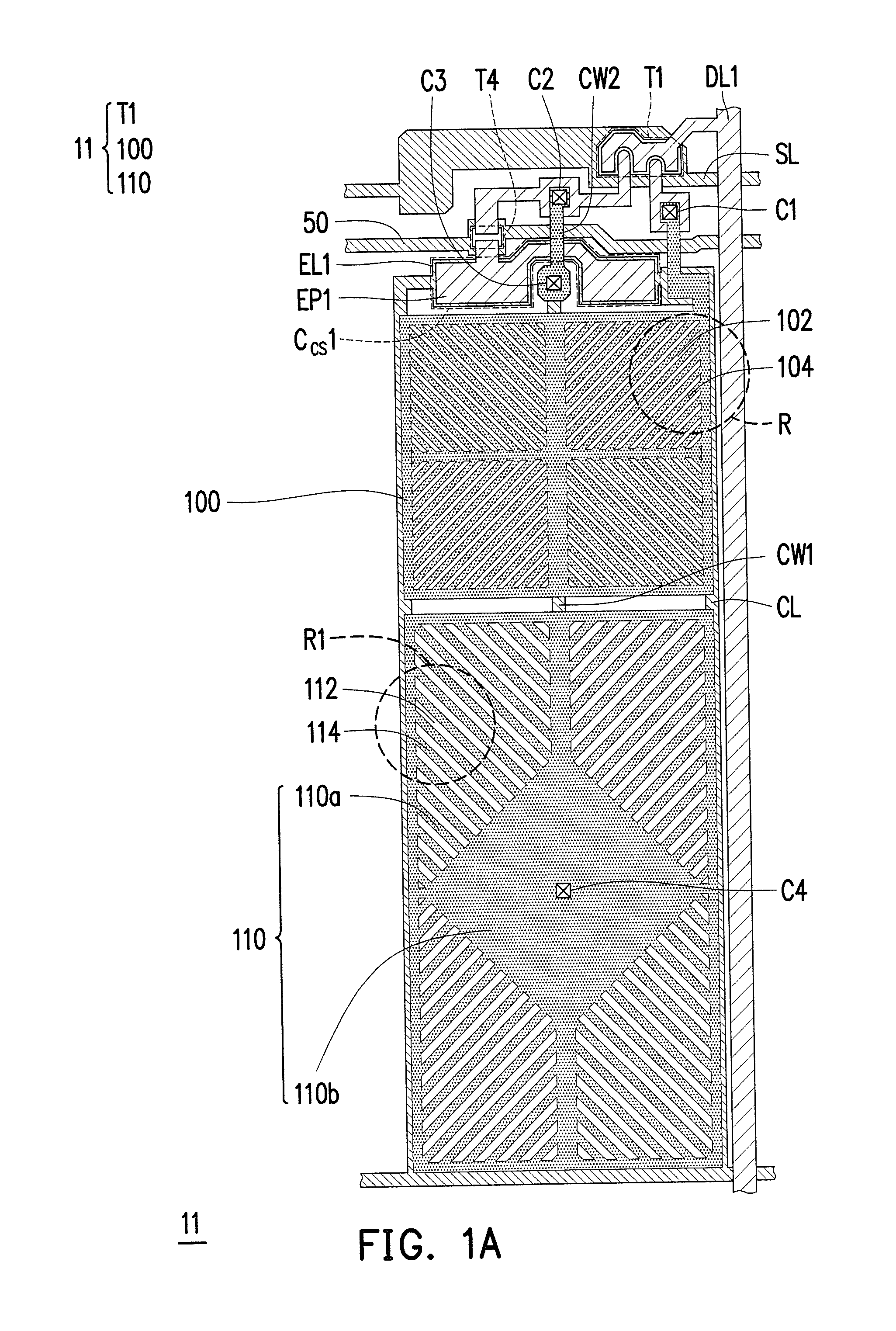
[0035]FIG. 1A is a schematic top view illustrating a pixel structure according to an embodiment of the invention. A pixel structure 11 of the present embodiment includes a control device T1, a main pixel electrode 100, and a sub-pixel electrode 110. Referring to FIG. 1A, the pixel structure 11 further includes: a scan line SL, a data line DL1, a signal line 50, a sharing switch device T4, wirings CW1˜CW2, a common line CL, a sharing capacitor Ccs1, a lower electrode EL1, a upper electrode EP1, and contact windows C1˜C4.

[0036]Extension directions of the scan line SL and the signal line 50 are different from an extension direction of the data line DL1. It is preferred that the extension directions of the scan line SL and the signal line 50 are perpendicular to the extension direction of the data line DL1. The scan line SL and the signal line 50 are, for example, located in the same layer or different layers, and the scan line SL and the signal line 50 are electrically isolated from on...


PUM


Abstract

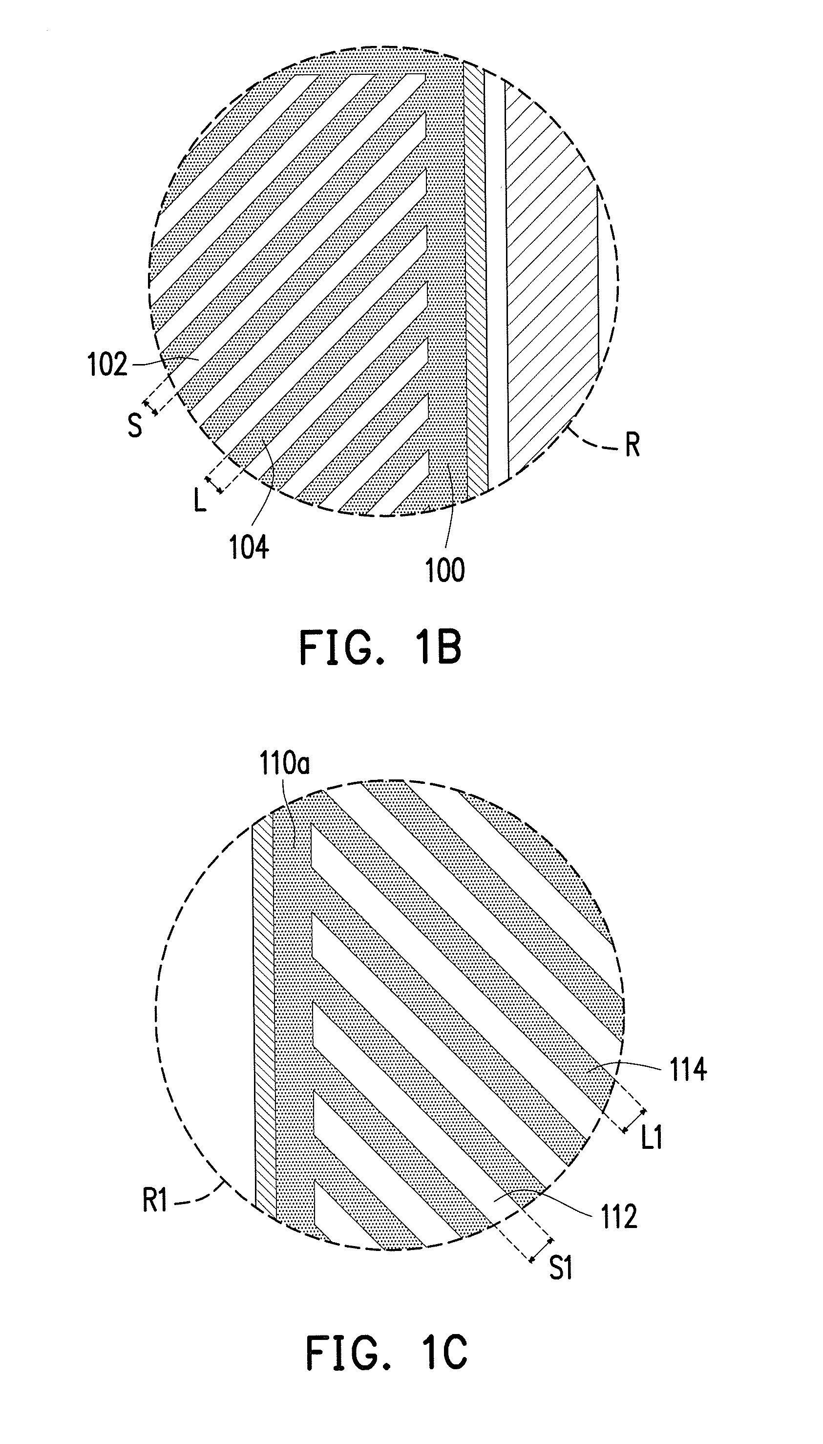
A pixel structure is provided. The pixel structure includes a control device, a main pixel electrode, and a sub pixel electrode. The main pixel electrode is electrically connected to the control device, and the main pixel electrode has a plurality of main pixel slits where the width thereof is S. The sub pixel electrode is electrically connected to the control device, and the sub pixel electrode has a first electrode pattern and a second electrode pattern. The first electrode pattern has a plurality of first slits where the width S1 thereof is equal to or greater than the width S of the main pixel slits. The second electrode pattern has no slits or has a plurality of second slits where the width S2 thereof is less than the width S of the main pixel slits. A pixel array including the pixel structure is also provided.

Description

CROSS-REFERENCE TO RELATED APPLICATION[0001]This application claims the priority benefit of Taiwan application serial no. 104116524, filed on May 22, 2015. The entirety of the above-mentioned patent application is hereby incorporated by reference herein and made a part of this specification.BACKGROUND OF THE INVENTION[0002]Field of the Invention[0003]The invention relaters to a pixel structure and a pixel array having the same.[0004]Description of Related Art[0005]As the LCD technology continuously progresses in a direction of providing a bigger display screen, the wide viewing techniques are being developed to improve the limited viewing angle inherent in a large-size display device. At the current stage, a commonly used wide viewing angle technique is a multi-domain vertical alignment (MVA) LCD panel.[0006]In the LCD panel, an alignment pattern is designed to divide liquid crystal molecules of a same pixel region into a plurality of different alignment domains to achieve a wide vi...

Claims


Application Information

Patent Timeline
IPC IPC(8): G02F1/1343G02F1/1362G02F1/1368
CPCG02F1/134309G02F1/1368G02F1/133707G02F1/13624G02F2001/134345G02F1/136286G02F1/134345
Inventor SHIH, CHIH-CHANGGONG, SHIN-MEILI, SHU-ENTIEN, KUN-CHENGLIAO, CHIEN-HUANG
Owner AU OPTRONICS CORP
Learn More