
Porous Glass Substrate For Displays And Method Of Manufacturing The Same

a technology of porous glass and display, which is applied in the direction of sustainable manufacturing/processing, final product manufacturing, transportation and packaging, etc., can solve the problems of complex manufacturing process, increased thickness of the substrate, and inability to apply silicone aerogel to an actual product, etc., to reduce manufacturing costs, reduce manufacturing costs, and prevent concave-convex structure

Active Publication Date: 2013-11-14
SAMSUNG CORNING PRECISION MATERIALS CO LTD
View PDF4 Cites 17 Cited by
  • Summary
  • Abstract
  • Description
  • Claims
  • Application Information

AI Technical Summary

Benefits of technology

The present invention provides a porous glass substrate for displays and a method of manufacturing the same that can improve the optical characteristics of OLED displays. The porous layer formed on the glass substrate has a lower refractive index than glass, which increases light extraction efficiency and reduces power consumption, leading to increased lifespan of the OLED. The manufacturing process of the porous glass substrate is easier and more cost-effective than existing methods. Additionally, the porous layer has a concave-convex pattern surface that promotes color mixing to reduce color shift in OLED displays.

Problems solved by technology

However, the silica aerogel has not been applied to an actual product, since the manufacturing process thereof is complicated, difficult and expensive.
In addition, the ability of the silica aerogel to be formed in a thin film is limited, thereby causing the increased thickness of the substrate.
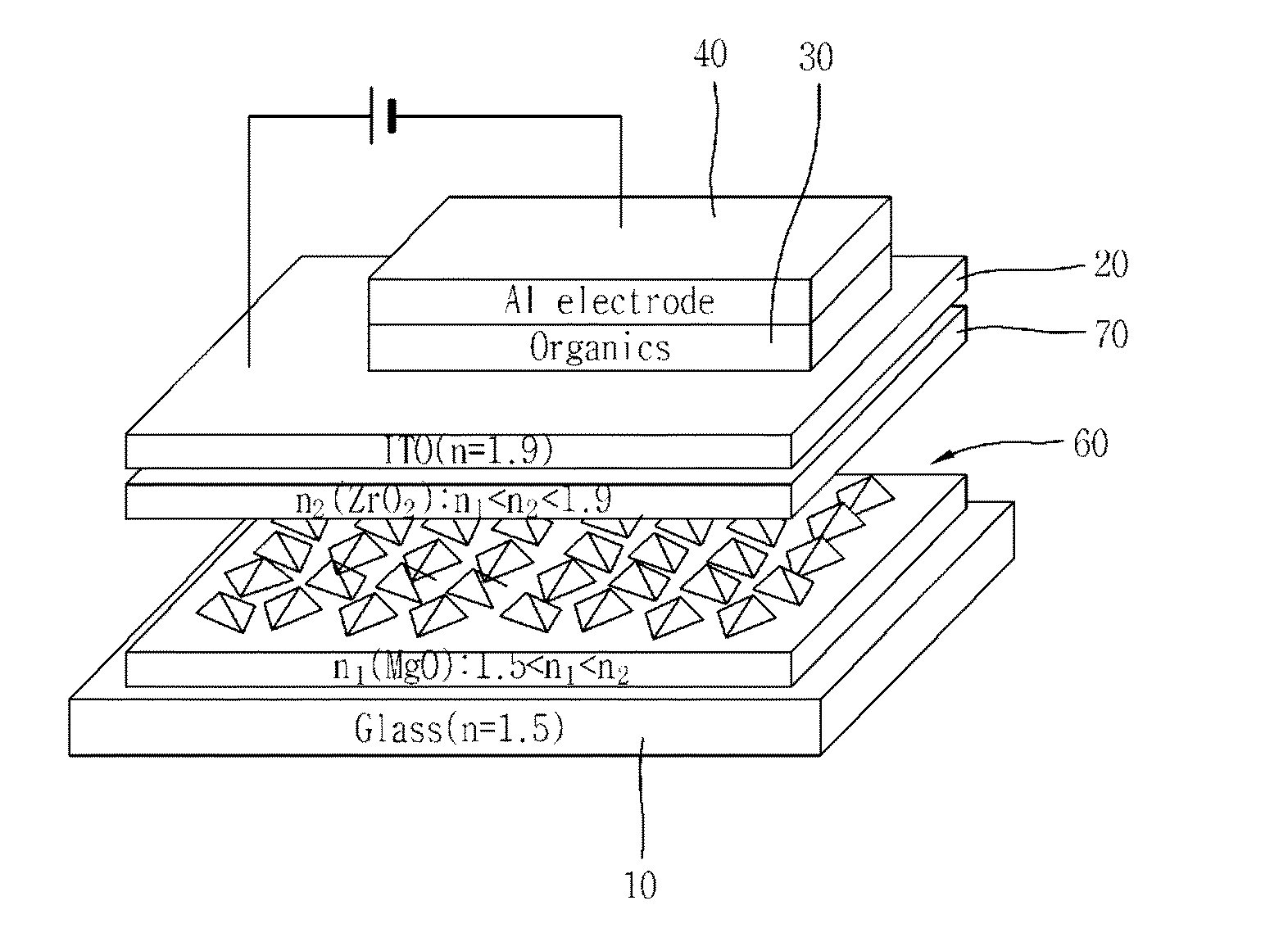
However, the process of completely flattening the concave-convex structure 60 using the thin flat film 70 having a thickness of several hundreds of nm is very difficult.
However, at present, it is very difficult to obtain a solution coating material that has a high refractive index, i.e. a refractive index that is equal to or greater than the refractive index of the ITO anode 20, and that satisfies process conditions for polycrystalline thin-film transistors, such as complicated conditions required on the surface of the OLED substrate and high-temperature processing.
However, this micro-cavity structure has the problem of causing color shift in which colors are changed depending on the position of a viewer within the viewing angle.

Method used


Image

  • Porous Glass Substrate For Displays And Method Of Manufacturing The Same
  • Porous Glass Substrate For Displays And Method Of Manufacturing The Same
  • Porous Glass Substrate For Displays And Method Of Manufacturing The Same

Examples


Embodiment Construction

[0046]Reference will now be made in detail to a porous glass substrate for displays and a method of manufacturing the same of the present invention, embodiments of which are illustrated in the accompanying drawings and described below, so that a person having ordinary skill in the art to which the present invention relates can easily put the present invention into practice.

[0047]Throughout this document, reference should be made to the drawings, in which the same reference numerals and signs are used throughout the different drawings to designate the same or similar components. In the following description of the present invention, detailed descriptions of known functions and components incorporated herein will be omitted when they may make the subject matter of the present invention unclear.

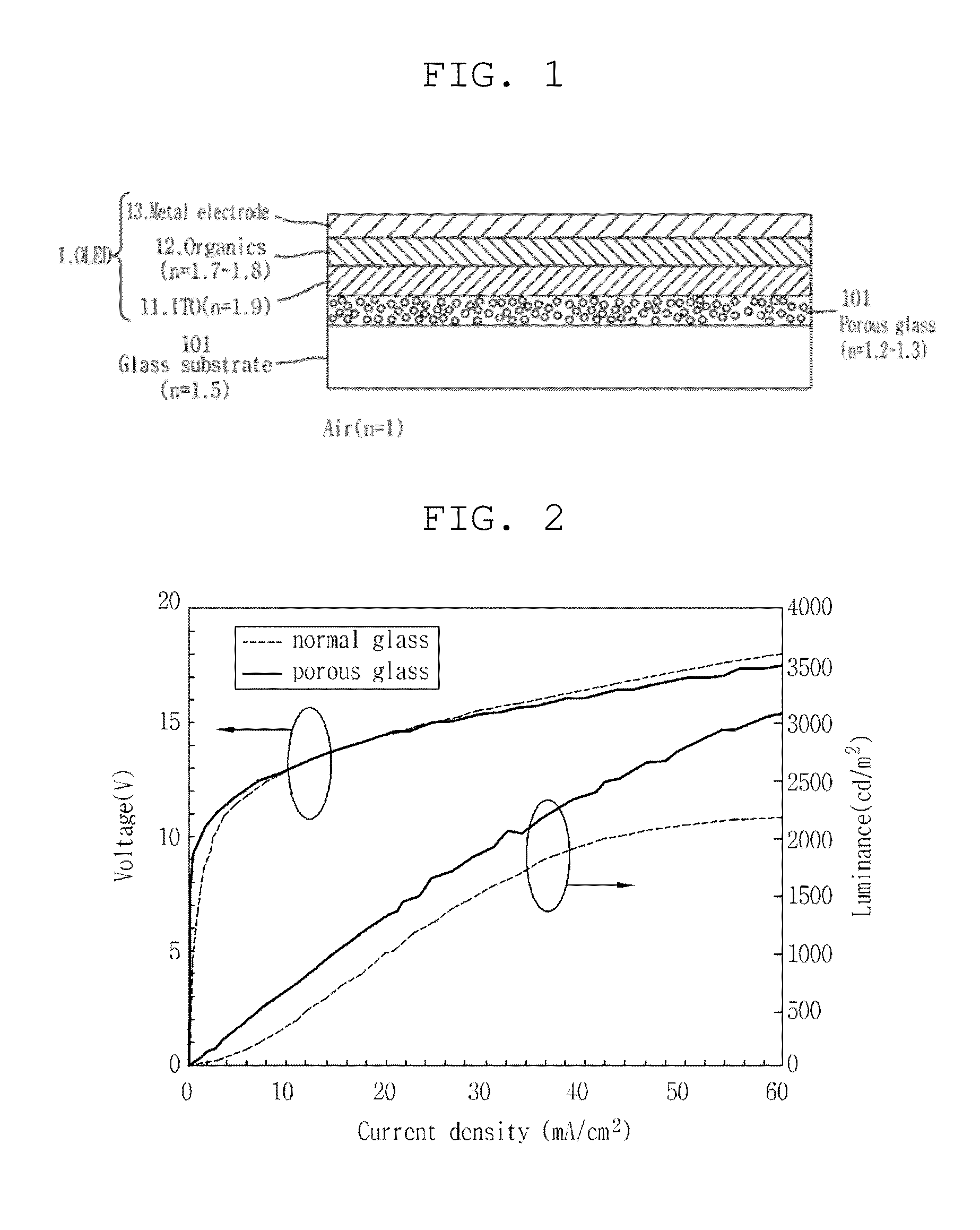
[0048]As shown in FIG. 1, a porous glass substrate 100 for displays according to an embodiment of the invention is one of opposing substrates used for an organic light-emitting device (OLED) 1. ...


PUM


Abstract

A porous glass substrate for displays and a method of manufacturing the same, with which the optical characteristics of a display such as an organic light-emitting device (OLED) can be improved. The porous glass substrate includes a glass substrate and a porous layer formed in at least one portion of one surface of the glass substrate and extending into the glass substrate, the refractive index of the porous layer being smaller than the refractive index of the glass substrate. The porous layer has a plurality of pores which is formed in the glass substrate such that at least one component of the glass substrate except for silicon dioxide (SiO2) is eluted from the glass substrate.

Description

CROSS REFERENCE TO RELATED APPLICATION[0001]The present application claims priority from Korean Patent Application Numbers 10-2012-0048903 and 10-2012-0142443 filed on May 9, 2012 and Dec. 10, 2012 respectively, the entire contents of which applications are incorporated herein for all purposes by this reference.BACKGROUND OF THE INVENTION[0002]1. Field of the Invention[0003]The present invention relates to a porous glass substrate for displays and a method of manufacturing the same, and more particularly, to a porous glass substrate for displays and a method of manufacturing the same, with which the optical characteristics of a display such as an organic light-emitting device (OLED) can be improved.[0004]2. Description of Related Art[0005]FIG. 6 is a cross-sectional and conceptual view depicting the light extraction efficiency of an organic light-emitting device (OLED) of the related art. As shown in FIG. 6, in the OLED of the related art, only about 20% of light generated is emitte...

Claims


Application Information

Patent Timeline
IPC IPC(8): H01L51/52
CPCH01L51/5268Y02E10/549Y10T428/24942Y10T428/24669Y02P70/50H10K77/10H10K59/879H10K59/877H10K50/854H10K50/858
Inventor PARK, SEONG- SIKYOO, JINAHKIM, TAE WONHAN, JINWOO
Owner SAMSUNG CORNING PRECISION MATERIALS CO LTD
Learn More