Liquid crystal display device

a liquid crystal display and display panel technology, applied in non-linear optics, instruments, optics, etc., can solve the problems of bending of the panel during the manufacturing process, and the panel is already bent when, so as to achieve the effect of not dropping the productivity of the liquid crystal display panel

Inactive Publication Date: 2016-12-01
JAPAN DISPLAY INC
View PDF7 Cites 15 Cited by
  • Summary
  • Abstract
  • Description
  • Claims
  • Application Information

AI Technical Summary

Benefits of technology

[0008]With a view to achieving higher productivity, liquid crystal display panels are generally manufactured as follows: A large number of liquid crystal panels are first formed on a mother substrate. Upon completion of the mother substrate, the individual liquid crystal panels are separated from that substrate. When separated from the mother substrate, each liquid crystal panel is shaped flat. If curved display devices are each manufactured by having a flat liquid crystal display panel bent upon installation onto the product, the productivity of the liquid crystal display panels will not drop.

Problems solved by technology

In this case, panels are already bent when they are in the manufacturing process.
In this case, too, the panels are bent in the manufacturing process.

Method used


Image

  • Liquid crystal display device
  • Liquid crystal display device
  • Liquid crystal display device

Examples


first embodiment

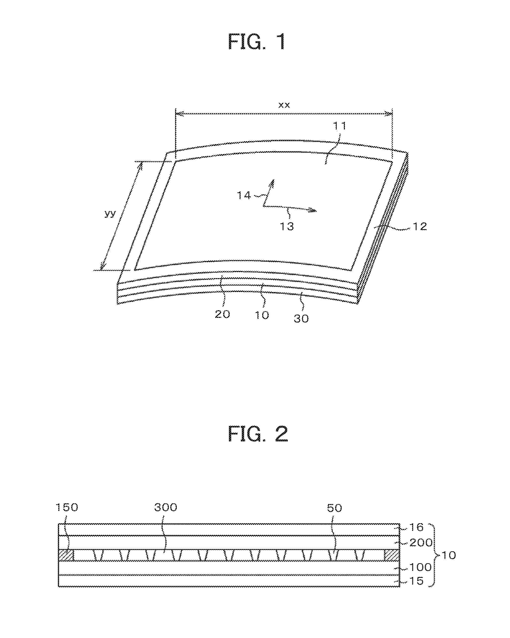
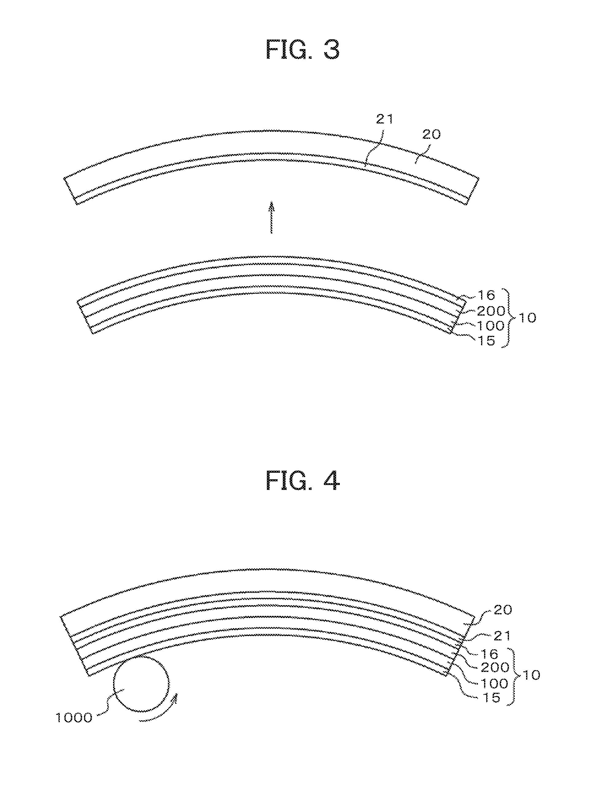
[0048]FIG. 1 is a perspective view of a curved liquid crystal display device. The display device in FIG. 1 is bent to have its convex screen facing the viewer. In FIG. 1, a protective panel 20 is disposed at the top, under which is a liquid crystal display panel 10. A backlight 30 is disposed at the back of the liquid crystal display panel 10. In FIG. 1, a frame area 12 is formed at the periphery of a rectangular display area 11. In FIG. 1, the long side dimension xx of the display area 11 is 230 mm, its short side dimension yy is 90 mm, and its radius of curvature is 500 mm, for example. FIG. 1 shows an example of a cylindrical curvature. This curvature has a curved axis 13 and an axis 14 perpendicular to the curved axis 13.

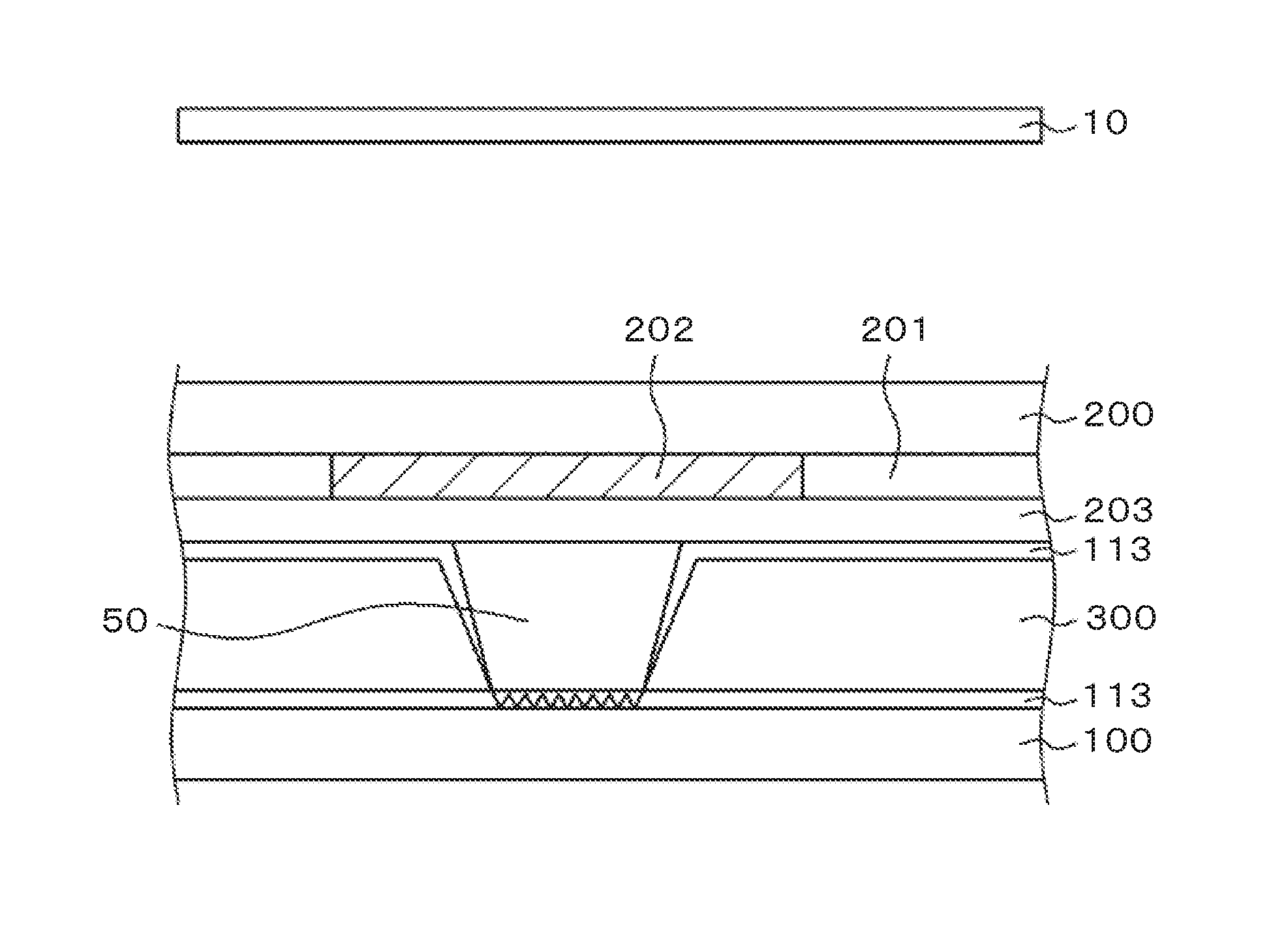
[0049]FIG. 2 is a cross-sectional view of a liquid crystal display panel. In FIG. 2, a counter substrate 200 is disposed opposite to a TFT substrate 100 having TFTs and pixel electrodes, among others, formed thereon in a matrix pattern. The TFT substrate 100 and...

second embodiment

[0082]FIG. 11 is a perspective view of a so-called cross spacer configured to determine the gap between the TFT substrate and the counter substrate in the second embodiment of the present invention. As shown in FIG. 11, the gap between the TFT substrate and the counter substrate is determined by a lower bar spacer 60 and an upper bar spacer 70 arranged to make up a cross shape, the lower bar spacer 60 having its long side dimension oriented in the crosswise direction of the TFT substrate, the upper bar spacer 70 having its long side dimension oriented in the longitudinal direction of the counter substrate. The lower bar spacer 60 and the upper bar spacer 70 are collectively called the cross spacer. In FIG. 11, the lower bar spacer 60 is disposed on a scanning line 1, and the upper bar spacer 70 is disposed in a position corresponding to a video signal line 2. Thus many cross spacers are disposed at the intersections between the scanning lines 1 and the video signal lines 2. Contrary...

third embodiment

[0099]As explained above in conjunction with the first and the second embodiments, the pixels formed on the TFT substrate 100 are displaced from the pixels formed on the counter substrate 200 when the liquid crystal display panel 10 is bent into a curved shape. If the center of each pixel on the TFT substrate 100 is made to coincide with the center of each pixel on the counter substrate 200 with the liquid crystal display panel 10 left flat, bending the liquid crystal display panel 10 into a curved shape displaces the pixel centers on the TFT substrate 100 from the pixel centers on the counter substrate 200, particularly at the periphery of the screen. The misalignment causes the light from the backlight having passed through the pixels on the TFT substrate 100 to pass not only through the intended color filter 201 but also through the adjacent color filter 201, bringing about a phenomenon called color mixture.

[0100]To prevent the problem of color mixture requires using a flat liqui...


PUM

PropertyMeasurementUnit
thicknessaaaaaaaaaa
thicknessaaaaaaaaaa
thicknessaaaaaaaaaa

Abstract

A liquid crystal display device has a liquid crystal display panel that includes a thin-film transistor (TFT) substrate having pixels formed thereon in a matrix pattern and a counter substrate, the two substrates having liquid crystal sandwiched therebetween to constitute a display area having a periphery encircled by a frame area. The display area has a first axis and a second axis perpendicular to the first axis. The liquid crystal display panel is curved along the first axis. The gap between the TFT substrate and the counter substrate is determined by columnar spacers formed on the counter substrate in a manner corresponding to positions of a black matrix over the counter substrate. The center of each of the columnar spacers is displaced in the first axis direction from the center of each of the corresponding positions of the black matrix.

Description

CLAIM OF PRIORITY[0001]The present application claims priority from Japanese Patent Application JP 2015-111322 filed on Jun. 1, 2015, the content of which is hereby incorporated by reference into this application.BACKGROUND OF THE INVENTION[0002]1. Field of the Invention[0003]The present invention relates to a display device. More particularly, the invention relates to a liquid crystal display device having a curved screen.[0004]2. Description of the Related Art[0005]Liquid crystal display devices are generally configured to have a thin-film transistor (TFT) substrate disposed opposite to a counter substrate with liquid crystal sandwiched therebetween, the TFT substrate having pixel electrodes and TFTs formed thereon in a matrix pattern for example. The display device forms an image by suitably controlling the light transmission factor of liquid crystal molecules for each pixel. The liquid crystal display device usually has a flat screen.[0006]However, some usages of the liquid crys...

Claims


Application Information

Patent Timeline
Patent Type & Authority Applications(United States)
IPC IPC(8): G02F1/1339G02F1/1335G02F1/1368
CPCG02F1/13394G02F2201/56G02F1/133512G02F1/1368G02F1/133305G02F1/13396
Inventor SHIINA, HIDEKINAGASAWA, JUNKOSHIMURA, MASATO
Owner JAPAN DISPLAY INC
Why Eureka
Try Eureka