Bowtie Nanoantennas and Methods of Using the Same

a nanoantenna and nanotechnology, applied in the field of metal nanoantenna fabrication and use, can solve the problems of limited pillar materials in fabrication techniques to metals or to a semiconductor substrate material, typically silicon, which is not optically transparen

Inactive Publication Date: 2016-12-22
THE BOARD OF TRUSTEES OF THE UNIV OF ILLINOIS
View PDF1 Cites 49 Cited by
  • Summary
  • Abstract
  • Description
  • Claims
  • Application Information

AI Technical Summary

Problems solved by technology

To date, however, known fabrication techniques have limited pillar materials to metals or to a semiconductor substrate material, typically silicon, which is not optically transparent.

Method used


Image

  • Bowtie Nanoantennas and Methods of Using the Same
  • Bowtie Nanoantennas and Methods of Using the Same
  • Bowtie Nanoantennas and Methods of Using the Same

Examples


Embodiment Construction

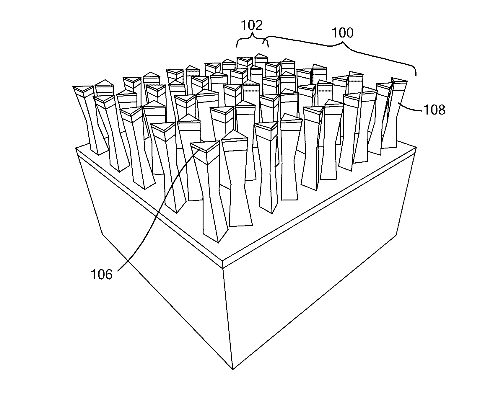
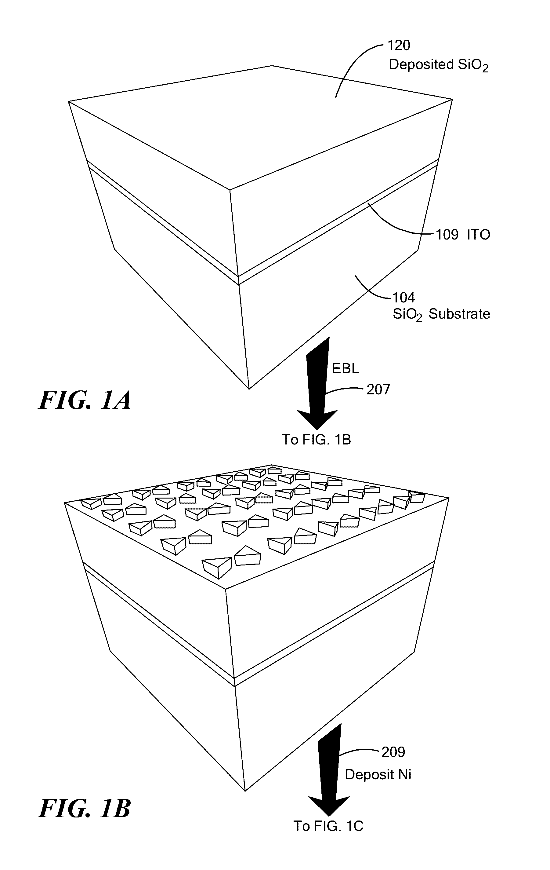
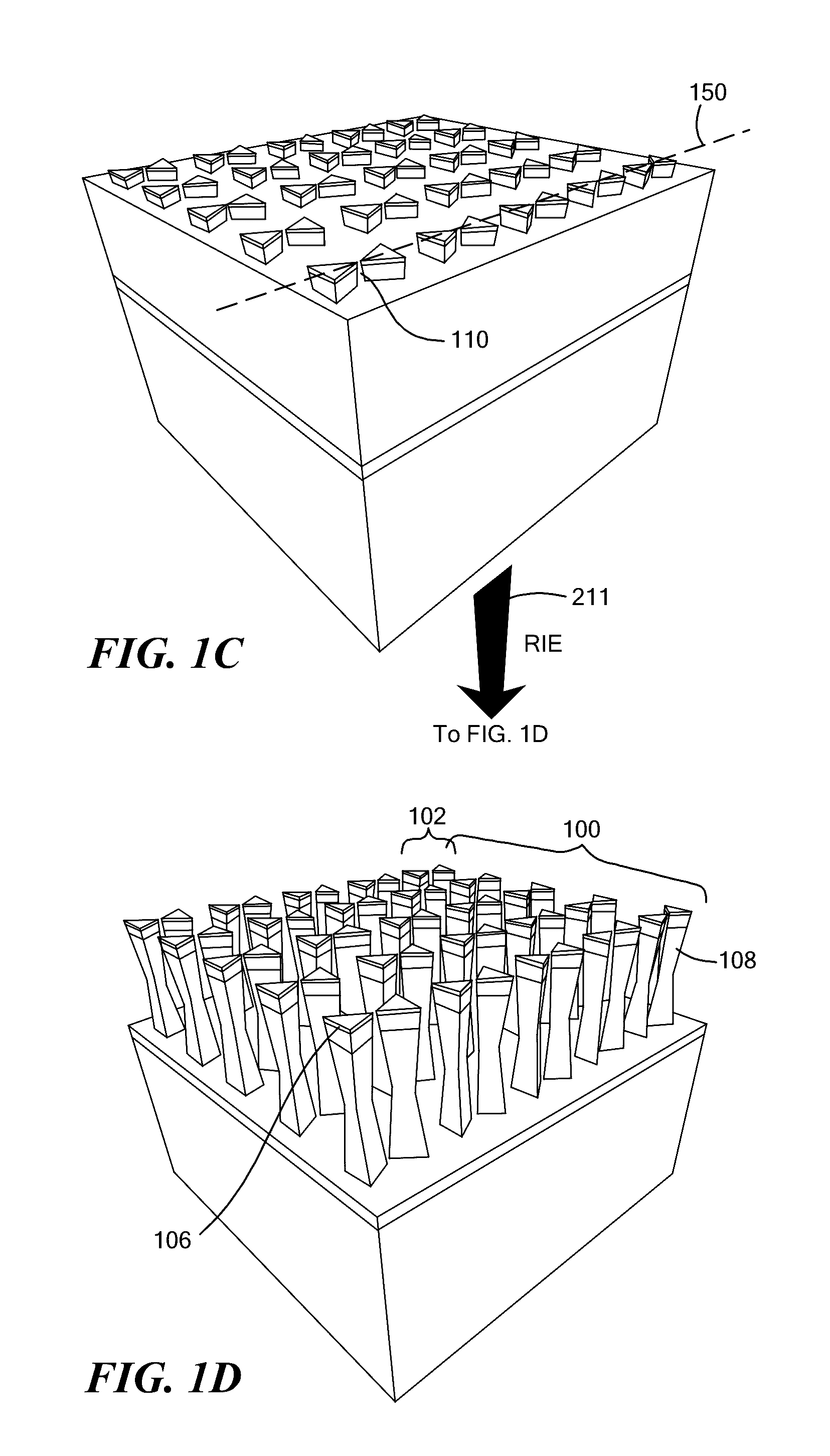
[0011]In accordance with embodiments of the invention, a structure is provided, having a surface and an array of pairs of pillars coupled to the substrate. The pillars are characterized by a thermal conductance less than 0.1 μW / deg, and have a metallic cap atop each pillar, wherein the metallic caps atop at least one neighboring pair of pillars are separated with respect to each other by no more than 50 nm. In an alternate embodiment of the invention, the pillars are substantially transparent in a visible portion of the spectrum and characterized by a ratio of height to thickness exceeding 2.0.

[0012]In accordance with other embodiments of the present invention, the metallic caps may be substantially triangular and the substrate surface may be substantially planar. The pillars may be substantially transparent in a specified portion of the electromagnetic spectrum.

[0013]The substrate and the pillars may be composed of an identical material, and a layer of conducting material may inter...


PUM

PropertyMeasurementUnit
thicknessaaaaaaaaaa
thicknessaaaaaaaaaa
thicknessaaaaaaaaaa

Abstract

A pillar-nanoantenna array structure is fabricated with a substrate to which pairs of pillars are coupled, where the pillars are characterized either by a thermal conductance less than 0.1 μW / deg or by transparency and a height exceeding thickness by at least a factor of two. Metallic caps atop a neighboring pair of pillars are separated by no more than 50 nm. An image-capture structure may be formed by modifying reflectance of a portion of the structure by heating of the portion by electromagnetic radiation. The array may be plastically deformed by raster scanning an electron beam across the array, exciting plasmon modes in the conducting particles thereby inducing a gradient force between neighboring conducting particles, and deforming neighboring pillars in such a manner as to vary the spacing separating neighboring conducting particles. A technique of plasmon-assisted etching provides for fabricating specified planar pattern of metal outside a cleanroom environment.

Description

[0001]The present application claims the priority of U.S. Provisional Patent Application 62 / 181,010, filed Jun. 16, 2015, and incorporated herein by reference.TECHNICAL FIELD[0002]The present invention relates to methods for fabricating and using plasmonic antennas, and, more particularly, to fabricating metal nanoantennas on insulating pillars.BACKGROUND ART[0003]The large near-field intensity gradients afforded by plasmonic nanotweezers have been an area of increasing interest, particularly in the field of lab-on-a-chip (LOC) devices. Indeed, the attributes of amplified optical forces and flexibility in shaping the optical potential energy landscape are well-suited for trapping nanoparticles, investigating colloidal dynamics, and manipulating biological species. In addition, arrays of gold bowtie nanoantennas (BNAs) are capable of yielding optical trapping efficiencies that are twenty times greater than conventional optical trapping, permitting the use of low input power densities...

Claims


Application Information

Patent Timeline
Patent Type & Authority Applications(United States)
IPC IPC(8): G02B21/32C03C15/00H01J37/30C03C23/00C03C17/36G03F7/20C03B23/00C03C17/34
CPCG02B21/32C03C2217/261C03C15/00C03C17/3482C03C23/004C03C17/3657C03C17/3649C03C17/3639C03C17/3636C03C17/3618G03F7/70H01J37/30C03C2217/228C03C2217/26C03C2217/255C03B23/00B82Y20/00B82Y30/00B82Y40/00C03C17/3417C03C17/36C03C2218/33G02B1/002
Inventor TOUSSAINT, KIMANI C.ROXWORTHY, BRIAN J.BHUIYA, ABDUL MONNAG
Owner THE BOARD OF TRUSTEES OF THE UNIV OF ILLINOIS
Why Eureka
Try Eureka