Structure and method for tunable memory cells including fin field effect transistors

a technology of fin field effect transistor and memory cell, applied in the field of memory cells, can solve the problem that coarse tuning may not be sufficient to achieve the effect of tunable memory cell

Active Publication Date: 2016-12-22
QUALCOMM INC
View PDF3 Cites 35 Cited by
  • Summary
  • Abstract
  • Description
  • Claims
  • Application Information

AI Technical Summary

Benefits of technology

[0010]One particular advantage provided by at least one of the disclosed aspects is one or more memory cells that include FinFETs and that are tunable during a design process to achieve target stability values and / or target writability values. For example, by selecting a width and a location of the dielectric region during a design process, the drive strengths of the FinFETs may be more finely tuned than the “coarse” tuning provided by selecting the number of fins in the FinFETs. Through the fine tuning, drive strength ratios that are fractional ratios may be achieved. In this manner, the one or more memory cells may achieve drive strength ratios associated with target stability values and / or target writability values.

Problems solved by technology

This coarse tuning may not be sufficient to achieve a particular drive strength ratio associated with a target stability or a target writability of an SRAM cell.

Method used


Image

  • Structure and method for tunable memory cells including fin field effect transistors
  • Structure and method for tunable memory cells including fin field effect transistors
  • Structure and method for tunable memory cells including fin field effect transistors

Examples


Embodiment Construction

[0021]Particular aspects of the present disclosure are described below with reference to the drawings. In the description, common features are designated by common reference numbers throughout the drawings.

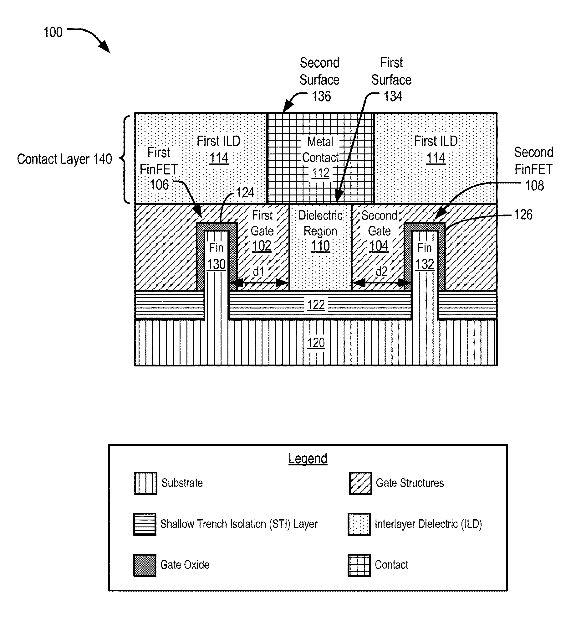
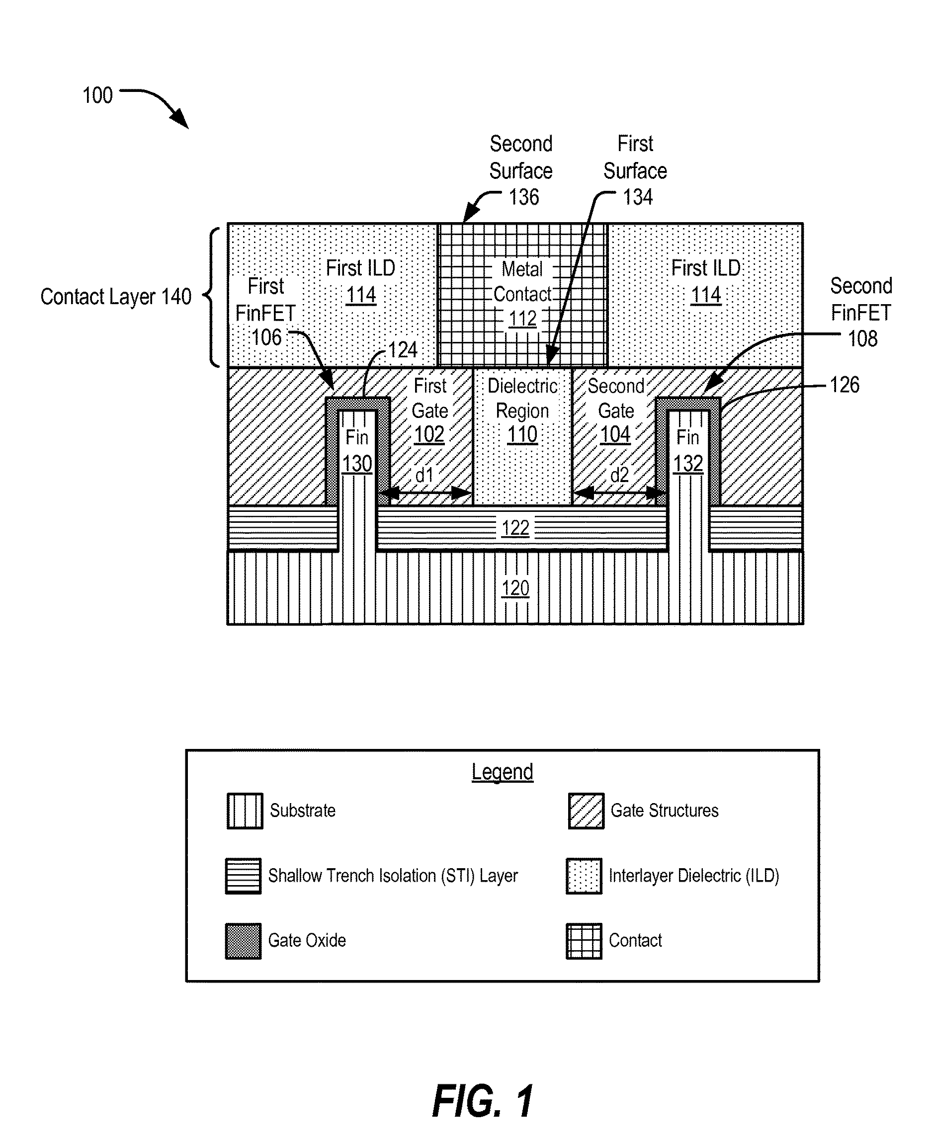
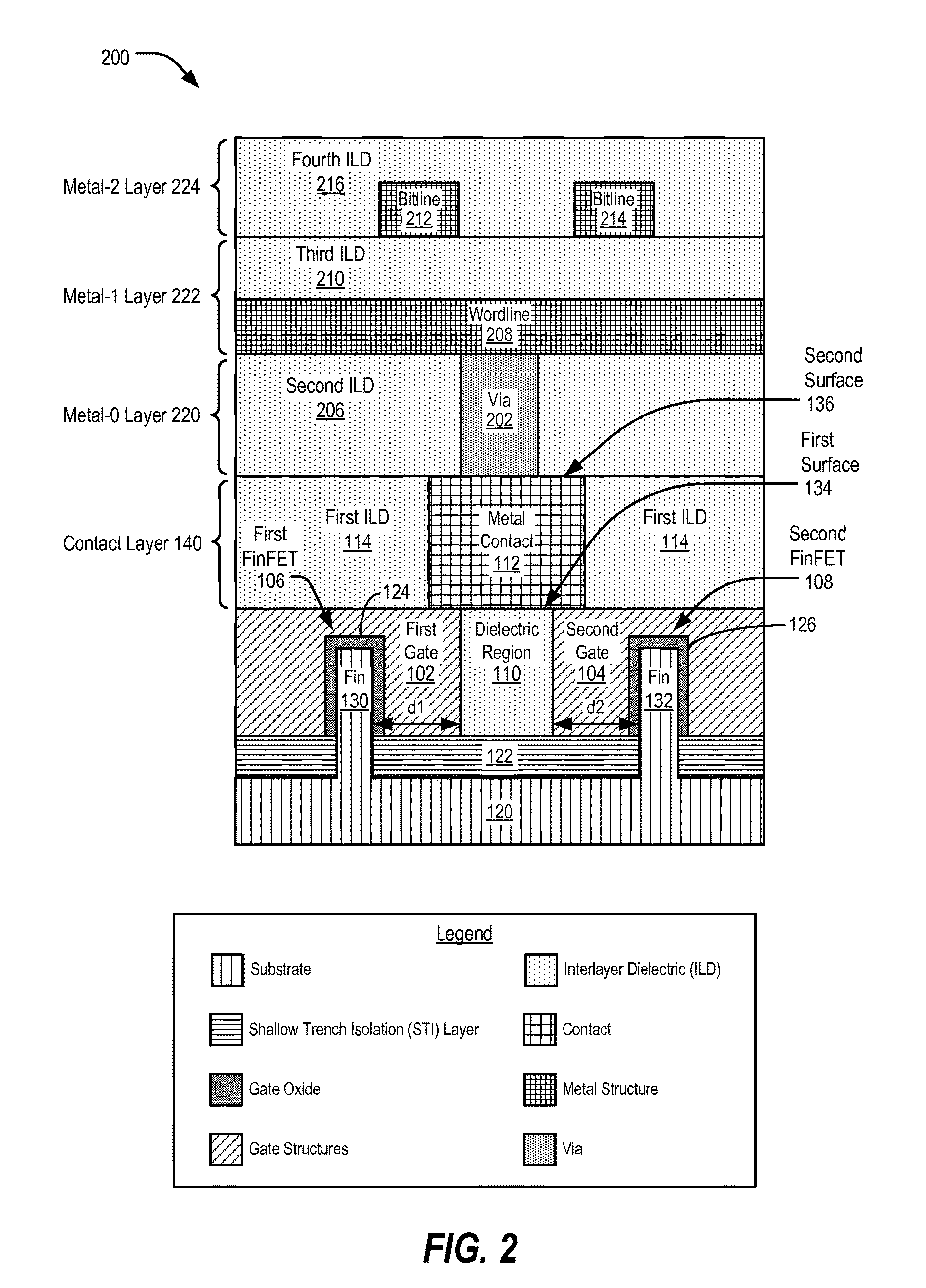
[0022]The present disclosure describes integrated circuits that include fin field-effect transistors (FinFETs) that are coupled to gate structures. The gate structures may be separated by a dielectric region, and a metal contact may electrically couple the gate structures together. The metal contact has a surface that is in contact with the dielectric region, the first gate structure, and the second gate structure (e.g., the metal contact is not in a higher metal layer of an integrated circuit). A width of the dielectric region and a position of the dielectric region relative to the gate structures may be selected during a design process to cause the FinFETs to have drive strengths that achieve drive strength ratios associated with a target stability value and / or a target writabil...


PUM


Abstract

In a particular aspect, an integrated circuit includes a first gate structure coupled to a first fin field effect transistor (FinFET) device. The integrated circuit includes a second gate structure coupled to a second FinFET device. The first gate structure and the second gate structure are separated by a dielectric region. The integrated circuit further includes a metal contact having a first surface that is in contact with the dielectric region, the first gate structure, and the second gate structure.

Description

I. FIELD[0001]The present disclosure is generally related to memory cells that include fin field-effect transistors.II. DESCRIPTION OF RELATED ART[0002]Advances in technology have resulted in smaller and more powerful computing devices. For example, a variety of portable personal computing devices, including wireless telephones such as mobile and smart phones, tablets and laptop computers are small, lightweight, and easily carried by users. These devices can communicate voice and data packets over wireless networks. Further, many such devices incorporate additional functionality such as a digital still camera, a digital video camera, a digital recorder, and an audio file player. Also, such devices can process executable instructions, including software applications, such as a web browser application, that can be used to access the Internet. As such, these devices can include significant computing and networking capabilities.[0003]Wireless devices may include static random access mem...

Claims


Application Information

Patent Timeline
Patent Type & Authority Applications(United States)
IPC IPC(8): H01L21/02H01L27/02G05B19/418H01L27/11
CPCH01L21/02H01L27/1104G05B2219/45031G05B19/418H01L27/0207H01L21/823431H01L21/823821H01L21/845H01L27/0886H01L27/1211H01L29/785H10B10/00H10B10/12H01L27/0924H01L21/76895H01L21/823475
Inventor YANG, HAININGLIU, YANXIANG
Owner QUALCOMM INC
Why Eureka
Try Eureka