Optical interconnect for switch applications

a technology of optical interconnection and switch, which is applied in the field of fiber optic communication, can solve the problems of the density and power consumption of the interconnect module being a bottleneck to the system, the cost of the optical transceiver can be substantial and sometimes even more costly than the switch, and the limitations of the architecture of the switch modul

Inactive Publication Date: 2016-12-29
T&S COMM
View PDF16 Cites 37 Cited by
  • Summary
  • Abstract
  • Description
  • Claims
  • Application Information

AI Technical Summary

Benefits of technology

[0014]These and other aspects of the invention are more fully comprehended upon review of this disclosure.

Problems solved by technology

Given the large number of lanes, the interconnect density and power consumption of the module can be a bottleneck to the system.
The cost of the optical transceivers can be substantial and sometimes even more costly than the switch.
As the switch ICs improve in performance, the switch modules are even more limited by the constraints of the architecture.
Thus the conventional switch is seriously limited by the architecture of a central switch IC connected to optical transceivers in the front panel, and the constraints are increasing with newer generations of switches.
A considerable amount of power may be consumed by the optical transceivers on the front panel, where airflow is often restricted.
Panel density—the size of the transceivers is such that one can only get a limited number on the front panel and thus only a limited bandwidth out of the front panel of the switch.

Method used


Image

  • Optical interconnect for switch applications
  • Optical interconnect for switch applications
  • Optical interconnect for switch applications

Examples


Embodiment Construction

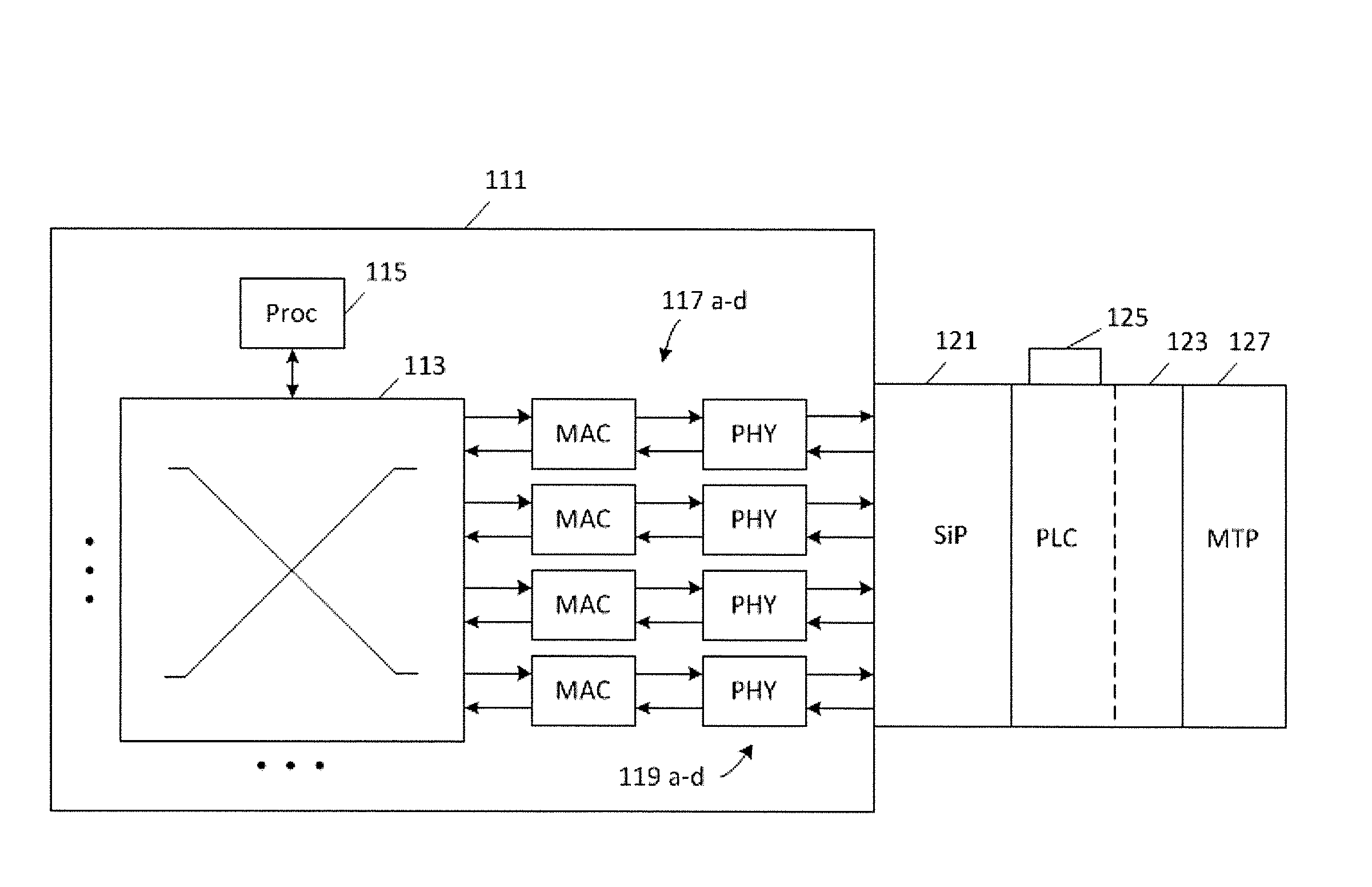
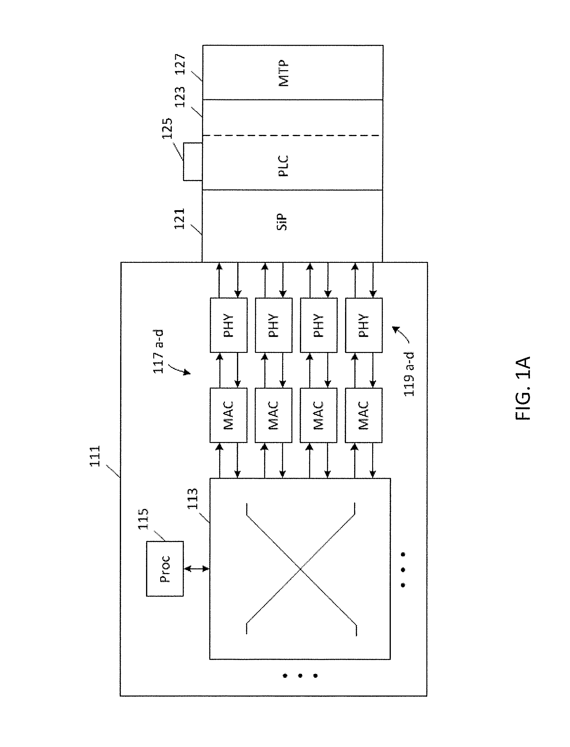
[0028]FIG. 1A is a block diagram of a switch module in accordance with aspects of the invention. The switch module includes a switch IC chip 111, a silicon photonics chip 121, and a PLC 123. A light source module 125 is coupled to the PLC, as is a connector 127 for fiber optic lines. The switch IC chip and the silicon photonics chip are electrically coupled so as to pass electrical data between themselves, while the silicon photonics chip and PLC are configured to pass optical data between themselves. The light source module, which for example may include a plurality of lasers or optical gain chips, is also optically coupled to the PLC.

[0029]In operation, the switch module receives and transmits optical data over the fiber optic lines. The received optical data is provided to the silicon photonics chip by the PLC, with the silicon photonics chip converting the received optical data to received electrical data. The received electrical data is passed to the switch IC chip, which deter...


PUM


Abstract

A switch module includes a switch integrated circuit (IC), a silicon photonics chips, and a planar lightwave circuits (PLCs).

Description

CROSS REFERENCE TO RELATED APPLICATION[0001]This application claims the benefit of the filing date of U.S. Provisional Patent Application No. 62 / 184,685, filed on Jun. 25, 2015, the disclosure of which is incorporated by reference herein.BACKGROUND OF THE INVENTION[0002]The present application relates generally to fiber optic communications and more particularly to switching devices having fiber optic connections.[0003]Much of our cloud based infrastructure is based on storage and processing of data by large numbers of servers in data centers. These servers are connected through a switch network in various configurations. A typical topology might be large groups of 96 servers in a rack connected to a top of rack (TOR) switch. These TOR switches are connected to an aggregation or leaf switch, which in turn is connected to a spine switch. The spine switches are interconnected to form a huge network where every server can connect with every other up and down various links in the system...

Claims


Application Information

Patent Timeline
Patent Type & Authority Applications(United States)
IPC IPC(8): H04Q11/00G02B6/12G02B6/42G02B6/43H04B10/25H04B10/80
CPCH04Q11/0005H04B10/2504H04B10/801G02B6/4274H04Q2011/0016G02B6/12021G02B6/4269H04Q2011/0052H04Q2011/0015G02B6/43G02B6/4285G02B6/12004H04B10/40
Inventor HEANUE, JOHNPEZESHKI, BARDIAAMSDEN, CHARLESSOLDANO, LUCAS
Owner T&S COMM
Why Eureka
Try Eureka