X-ray inspection apparatus for inspecting semiconductor wafers

Active Publication Date: 2017-01-12
NORDSON CORP
View PDF2 Cites 7 Cited by
  • Summary
  • Abstract
  • Description
  • Claims
  • Application Information

AI Technical Summary

Benefits of technology

[0130]The benefit of a sample support in accordance with this aspect of the invention is that it does not give rise to significant contrast changes in x-ray images resulting from x-rays that have passed through t

Problems solved by technology

Fabrication plants require many expensive devices to function.
Any time that a fabrication plant is not operating, for example for maintenance of a machine within the plant, is very undesirable.
While optical inspection of surface features can be achieved rapidly and reliably, inspection of internal f

Method used


Image

  • X-ray inspection apparatus for inspecting semiconductor wafers
  • X-ray inspection apparatus for inspecting semiconductor wafers
  • X-ray inspection apparatus for inspecting semiconductor wafers

Examples


Embodiment Construction

[0176]X-Ray Inspection System Components

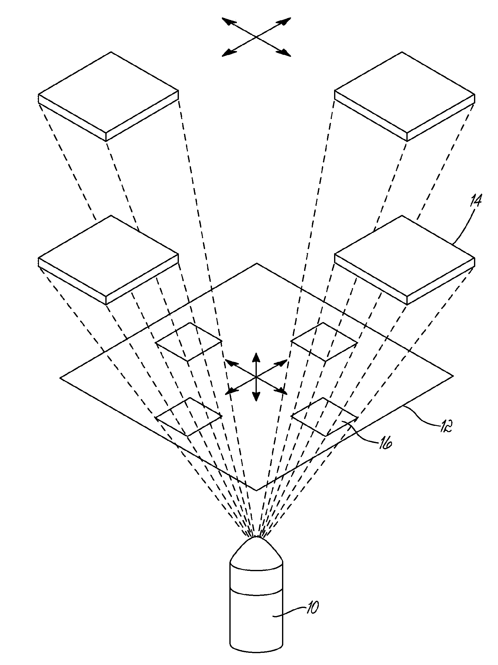
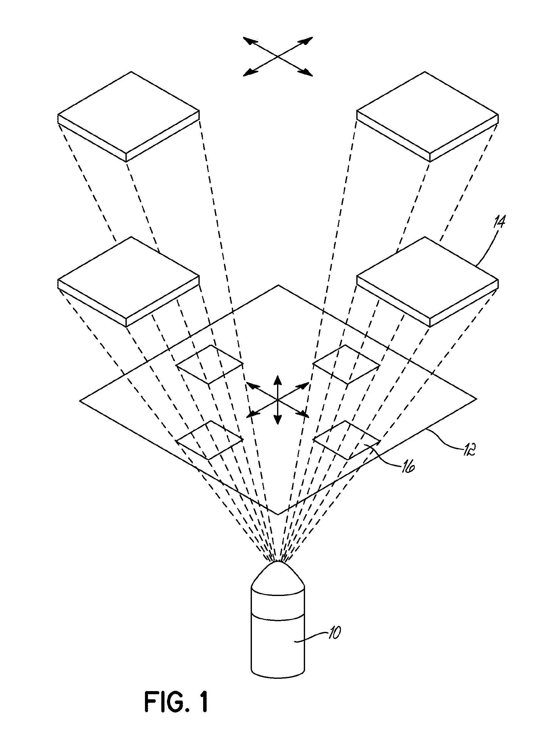
[0177]FIG. 1 is a schematic illustration of the basic elements of an x-ray imaging system. The system shown in FIG. 1 comprises an x-ray source 10, which in this system is held stationary, a moveable sample support 12 and a moveable detector 14. X-rays from the x-ray source 10 pass through the support and any sample mounted on the sample support, and impinge on the detector 14. FIG. 1 illustrates the areas 16 on the sample support corresponding to the field of view of the detector 14. The field of view of the detector is selected by a user by the relative positioning of the detector 14, sample support 12 and x-ray source 10 so that the sample, or an area of the sample, is within the field of view of the detector. The detector can move to different imaging positions so that different projections can be taken through samples on the sample support. In this context, a different projection means that the x-rays pass through the sample on the suppor...


PUM


Abstract

An x-ray inspection system includes a cabinet including an x-ray source, a sample support supporting a sample to be inspected, and an x-ray detector. The system further includes an air mover configured to force air into the cabinet through an air inlet in the cabinet above the sample support. The air mover and cabinet are configured to force air through the cabinet from the air inlet past the sample support to an air outlet in the cabinet below the sample support. The cabinet may be constructed to provide an x-ray shield. The x-ray inspection system can be used in a clean room environment to inspect items such as semiconductor wafers.

Description

FIELD OF THE INVENTION[0001]The invention relates to x-ray inspection apparatus and in particular to an apparatus and method suitable for inspecting a semiconductor wafer during the processing of the semiconductor wafer to produce integrated circuits. However, aspects of the invention relate to x-ray inspection systems in general and can be applied to systems for inspecting any type of sample.BACKGROUND TO THE INVENTION[0002]Fabricating integrated circuits is a multiple-step sequence of photolithographic and chemical processing steps during which electronic circuits are gradually created on a wafer made of pure semiconductor, typically silicon. The entire manufacturing process, from start to finish, takes six to eight weeks and is performed in highly specialized facilities referred to as fabrication plants. Fabrication plants require many expensive devices to function. Estimates put the cost of building a new fabrication plant over one billion U.S. dollars, with values as high as $3...

Claims


Application Information

Patent Timeline
IPC IPC(8): H01L21/66G01N23/04
CPCH01L22/12G01N23/04G01N2223/6462G01N2223/6113G01N2223/309H01L21/67288H01L21/681H01L21/6838G01N2223/6116G01N23/043
Inventor TINGAY, JOHNWALKER, WILLIAM T.STEWART, KATE
Owner NORDSON CORP
Why Eureka
Try Eureka