Planar optical waveguide device, DP-QPSK modulator, coherent receiver, and polarization diversity

Active Publication Date: 2017-01-19
FUJITSU OPTICAL COMPONENTS LTD
View PDF1 Cites 16 Cited by
  • Summary
  • Abstract
  • Description
  • Claims
  • Application Information

AI Technical Summary

Benefits of technology

[0050]As described above, according to the aspects of the invention, it is possible to provide a planar optical waveguide device capable of reducing a device len

Problems solved by technology

However, in an optical modulation method for high-speed communication including such a polarization multiplexing method, a structure of an optical modulator becomes complicated, which causes a problem in that the size of an apparatus becomes large and the manufacturing cost increases.
However, the optical modulator including the polarization multiplexing method using the planar optical waveguide device has the following problems.
However, in a case where an optical modulation operation is performed with respect to polari

Method used


Image

  • Planar optical waveguide device, DP-QPSK modulator, coherent receiver, and polarization diversity
  • Planar optical waveguide device, DP-QPSK modulator, coherent receiver, and polarization diversity
  • Planar optical waveguide device, DP-QPSK modulator, coherent receiver, and polarization diversity

Examples


Example

First Embodiment

Planar Optical Waveguide Device

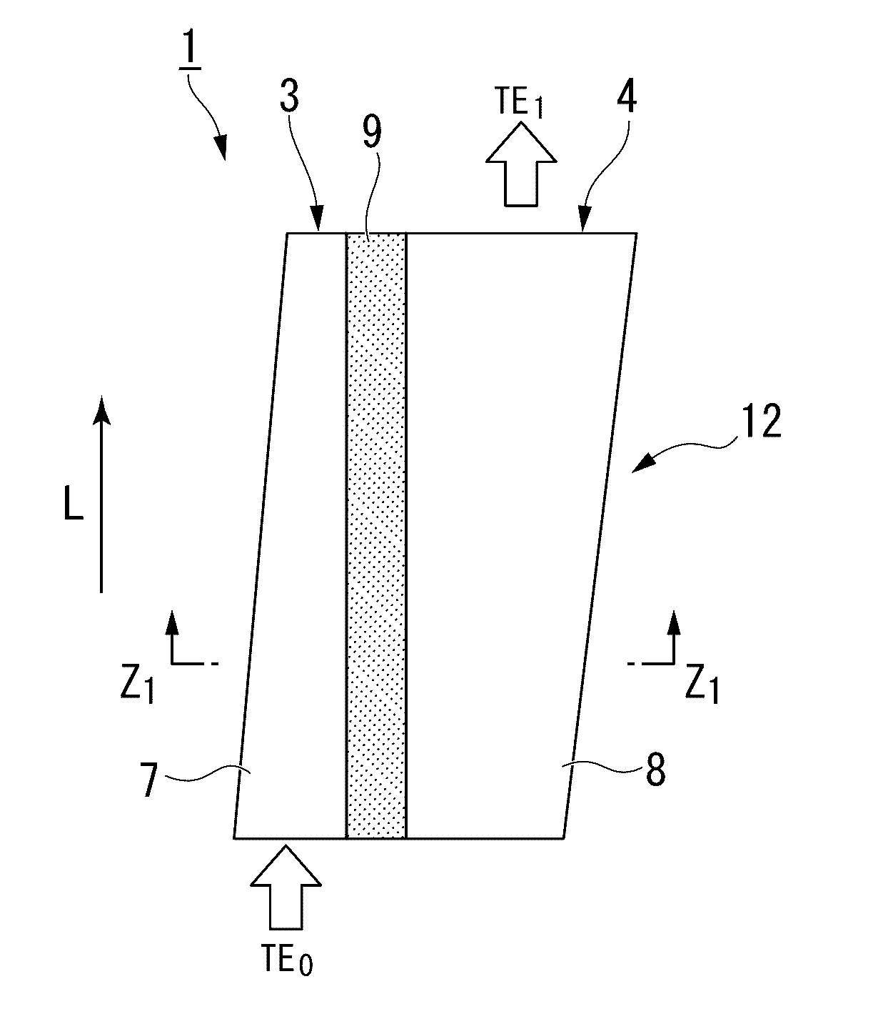
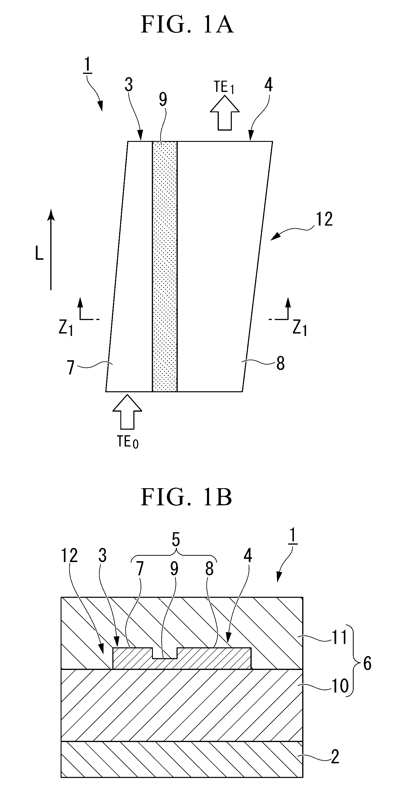
[0214]Next, a planar optical waveguide device 101 shown in FIGS. 32A and 32B will be described as a first embodiment of the invention. FIG. 32A is a plan view showing the planar optical waveguide device 101, and FIG. 32B is a cross-sectional view of the planar optical waveguide device 101 in an enclosure part C indicated by a broken line in FIG. 32A. Further, in the following description, a description of the same portions as in the planar optical waveguide device 1 shown in FIGS. 1A and 1B will not be repeated, and are given the same reference numerals in the drawings.

[0215]The planar optical waveguide device 101 shown in FIGS. 32A and 32B has a configuration corresponding to the planar optical waveguide device 1 in the enclosure part C. Further, the planar optical waveguide device 101 includes a first linear waveguide 102 connected to an input side of a first waveguide 3, a first bending waveguide 103 connected to an output side of th...

Example

Second Embodiment

Planar Optical Waveguide Device

[0227]Next, a planar optical waveguide device 101A shown in FIGS. 33A, 33B, and 33C will be described as a second embodiment. FIG. 33A is a plan view showing the planar optical waveguide device 101A. FIG. 33B is a plan view showing a tapered waveguide 106 provided in the planar optical waveguide device 101A. FIG. 33C is a plan view showing a modification example of a taper waveguide 107.

[0228]The planar optical waveguide device 101A of this embodiment shown in FIG. 33A has substantially the same configuration as that of the planar optical waveguide device 101, except that shapes of slab portions 9C to 9F are different outside the enclosure part C.

[0229]The planar optical waveguide device 101A of this embodiment has a configuration in which the tapered waveguide 106 as shown in FIG. 33B is connected to a first linear waveguide 102, a first bending waveguide 103, a second bending waveguide 104, and a second linear waveguide 105.

[0230]In ...

Example

Third Embodiment

Planar Optical Waveguide Device

[0237]Next, a planar optical waveguide device 101C shown in FIGS. 34A and 34B will be described as a third embodiment. FIG. 34A is a plan view showing the planar optical waveguide device 101C, and FIG. 34B is a cross-sectional view of the planar optical waveguide device 101C based on line segment Z2-Z2 shown in FIG. 34A. Further, in the following description, a description of the same portions as in the planar optical waveguide device 1 will not be repeated, and are given the same reference numerals in the drawings.

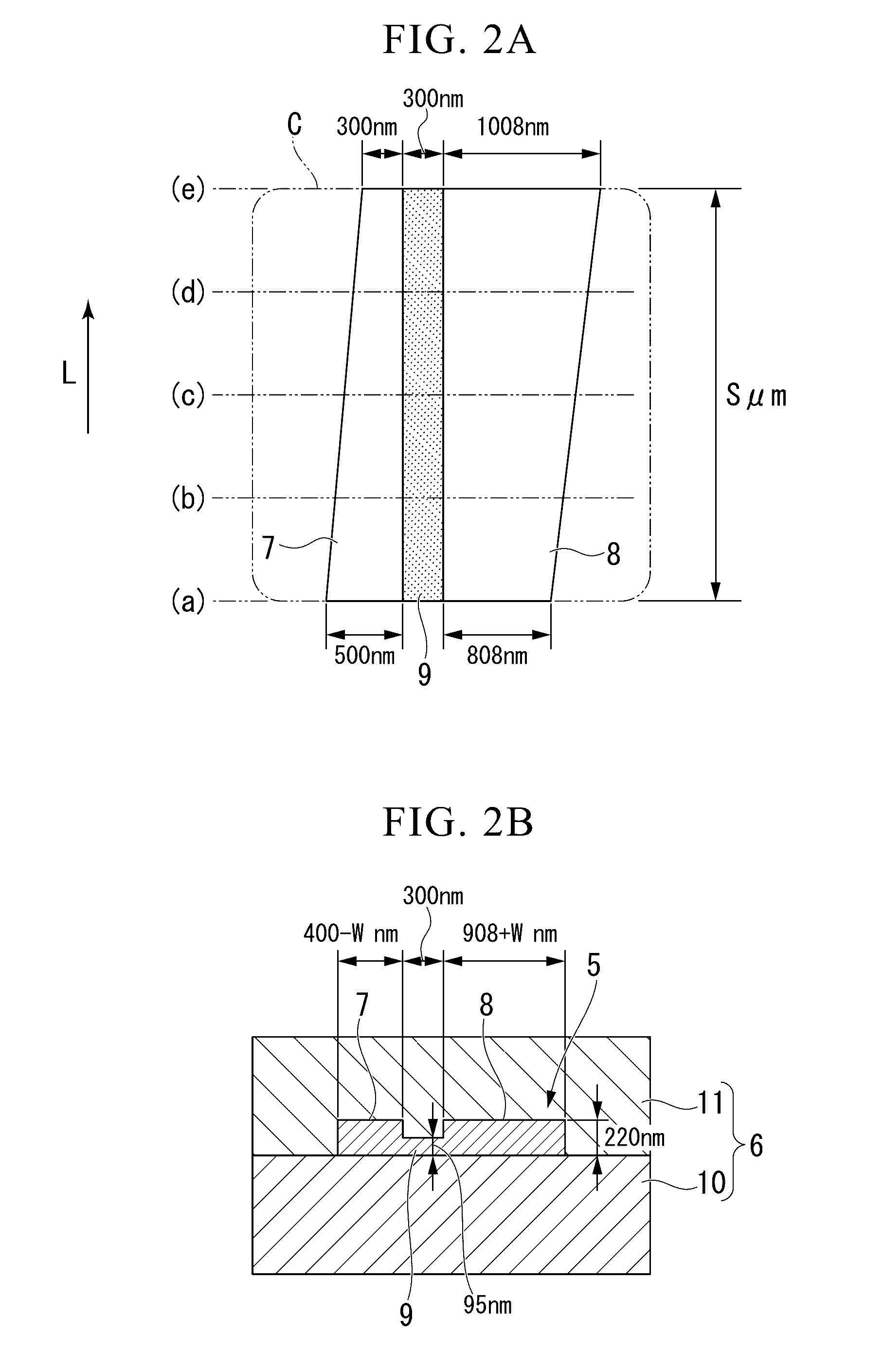
[0238]The planar optical waveguide device 1 has a configuration in which the width of the slab portion 9 is uniform in the length direction of the first rib portion 7 and the second rib portion 8, but the planar optical waveguide device 101C shown in FIGS. 34A and 34B has a configuration in which the width of the slab portion 9 changes along the length direction of the first rib portion 7 and the second rib portion 8.

[0239]Sp...


PUM


Abstract

A planar optical waveguide device includes: a substrate; a core that forms a first waveguide and a second waveguide that are arranged in parallel on the substrate; and a cladding that covers the core and has a refractive index smaller than that of the core. The core includes a first rib portion that forms the first waveguide, a second rib portion that forms the second waveguide, and a slab portion that is provided only on one side of the first rib portion and the second rib portion in a width direction to have a thickness smaller than the thicknesses of the first rib portion and the second rib portion and is shared between the first rib portion and the second rib portion.

Description

CROSS REFERENCE TO RELATED APPLICATIONS[0001]This application is a continuation application based on a PCT Patent Application No. PCT / JP2015 / 053770, filed Feb. 12, 2015, whose priority is claimed on Japanese Patent Application No. 2014-077232, filed on Apr. 3, 2014, the entire content of which are hereby incorporated by reference.BACKGROUND OF THE INVENTION[0002]Field of the Invention[0003]The present invention relates to a planar optical waveguide device.[0004]Description of the Related Art[0005]In recent years, the amount of information transmitted through optical communications has been steadily increasing. To cope with the increase in the amount of information, measures such as increasing a transmission speed, increasing the number of channels based on wavelength multiplexing communication, or the like have advanced. Particularly, in the next generation 100 Gbps digital coherent transmission technology for high speed information communication, a polarization multiplexing method ...

Claims


Application Information

Patent Timeline
IPC IPC(8): G02B6/126G02B6/122G02B6/125
CPCG02B6/126G02B2006/12097G02B6/1228G02B6/125G02B6/122G02B6/14
Inventor OKA, AKIRA
Owner FUJITSU OPTICAL COMPONENTS LTD
Why Eureka
Try Eureka