Chip-type electronic component

a technology of electronic components and chips, applied in the direction of capacitor details, electrical appliances, capacitors, etc., can solve the problems of difficult to prevent and achieve the effect of preventing the generation of unnecessary stray capacitan

Active Publication Date: 2017-01-19
MURATA MFG CO LTD
View PDF1 Cites 1 Cited by
  • Summary
  • Abstract
  • Description
  • Claims
  • Application Information

AI Technical Summary

Benefits of technology

[0007]In the chip-type electronic component 100 of the known technique as described above, unnecessary stray capacitance between the inner electrodes 102 and other electrode members arranged on upper and lower sides of the inner electrodes 102, that is, unnecessary stray capacitance between the inner electrodes 102 and the other electrode members in a thickness direction of the chip-type electronic component 100 can be reduced. However, it is difficult to prevent the generation of unnecessary stray capacitance between the inner electrodes 102 and other electrode members disposed in a direction orthogonal to the above-mentioned thickness direction.

Problems solved by technology

However, it is difficult to prevent the generation of unnecessary stray capacitance between the inner electrodes 102 and other electrode members disposed in a direction orthogonal to the above-mentioned thickness direction.

Method used


Image

  • Chip-type electronic component
  • Chip-type electronic component
  • Chip-type electronic component

Examples


first embodiment

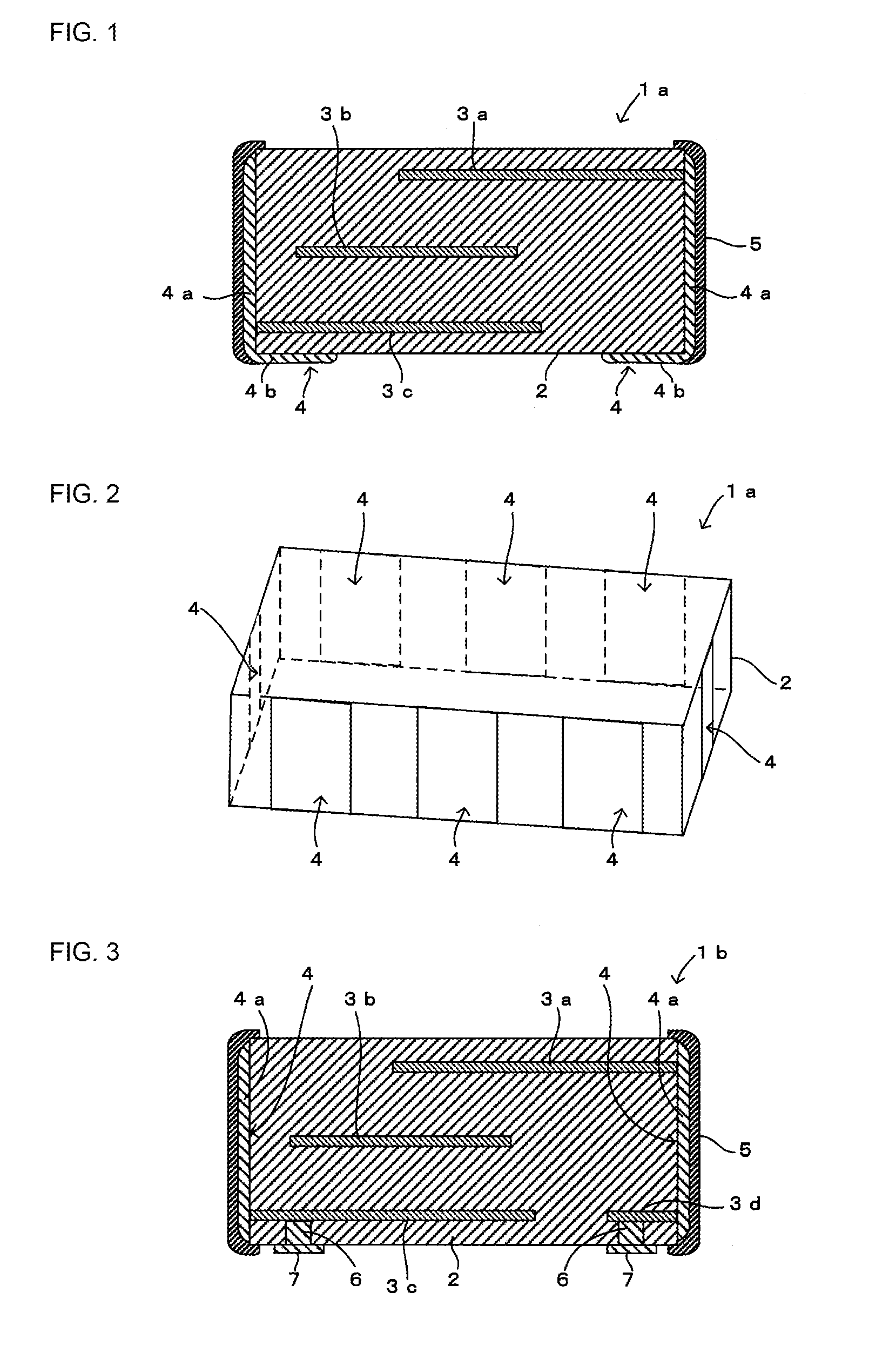
[0027]A chip-type electronic component 1a according to a first embodiment of the present disclosure will be described with reference to FIGS. 1 and 2. FIG. 1 is a cross-sectional view of the chip-type electronic component 1a, and FIG. 2 is a perspective view of the chip-type electronic component 1a. Note that in FIG. 2, a cover layer 5 is not illustrated.

[0028]The chip-type electronic component 1a according to the present embodiment includes, as shown in FIG. 1, a chip element assembly 2 having an upper surface, a lower surface, and a side surface; a plurality of inner electrodes 3a, 3b, and 3c formed inside the chip element assembly 2; a plurality of side surface electrodes 4 (each of which corresponds to “first side-surface electrode” of the present disclosure) formed on the side surface of the chip element assembly 2; and a cover layer 5 that is so provided as to cover the side surface of the chip element assembly 2 on which the side surface electrodes 4 are formed. This chip-typ...

second embodiment

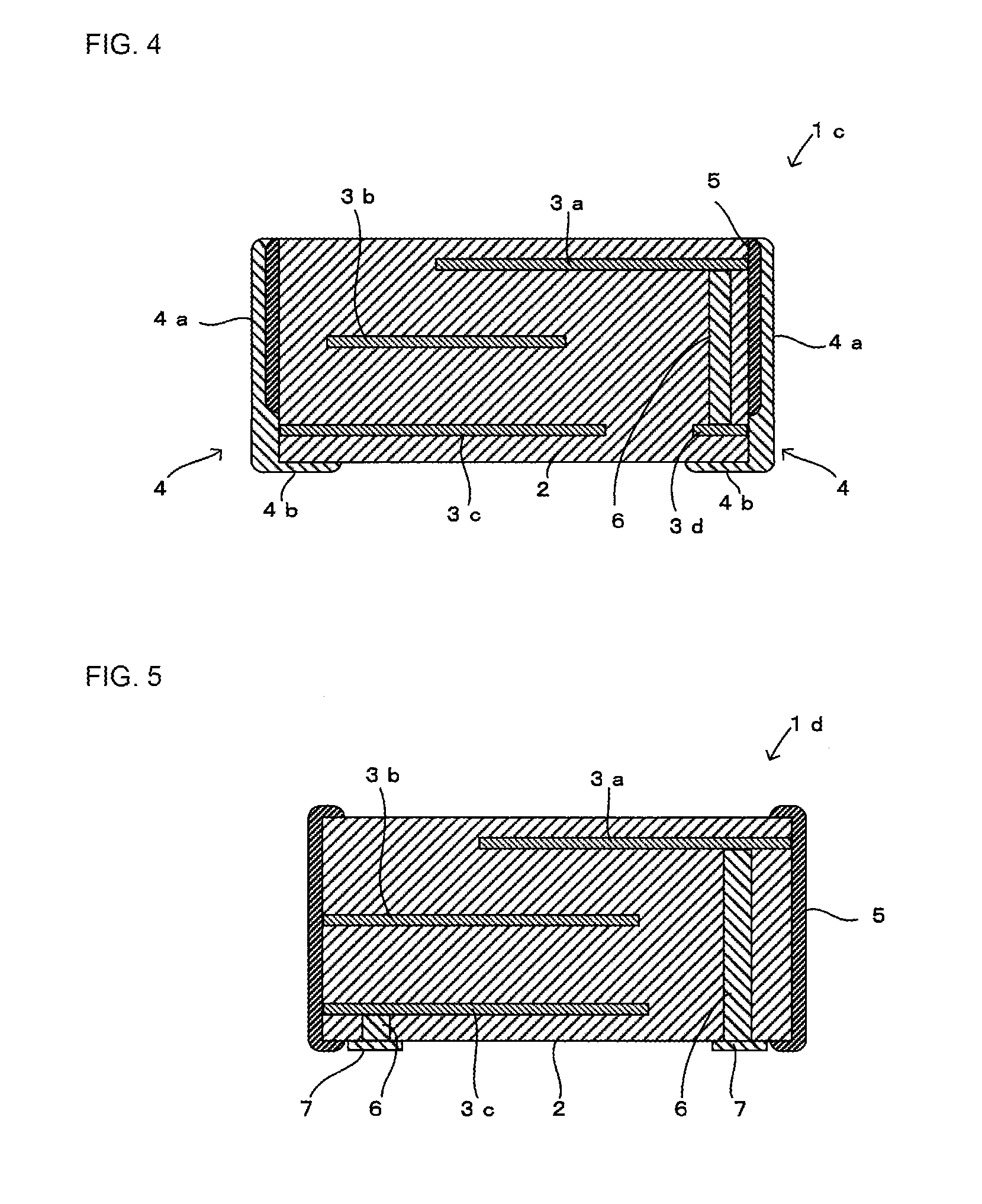
[0038]A chip-type electronic component 1b according to a second embodiment of the present disclosure will be described with reference to FIG. 3. Note that FIG. 3 is a cross-sectional view of the chip-type electronic component 1b.

[0039]The chip-type electronic component 1b according to the present embodiment differs from the chip-type electronic component 1a of the first embodiment having been discussed with reference to FIGS. 1 and 2 in a point that each of the side surface electrodes 4 does not have the extended section 4b, but only has the side surface section 4a, as shown in FIG. 3. Because other constituent elements are the same as those of the chip-type electronic component 1a of the first embodiment, the same reference signs are assigned thereto and description thereof is omitted.

[0040]In this case, in place of the extended sections 4b of the side surface electrodes 4, a plurality of land electrodes 7 for outer connection are formed on the lower surface of the chip element as...

third embodiment

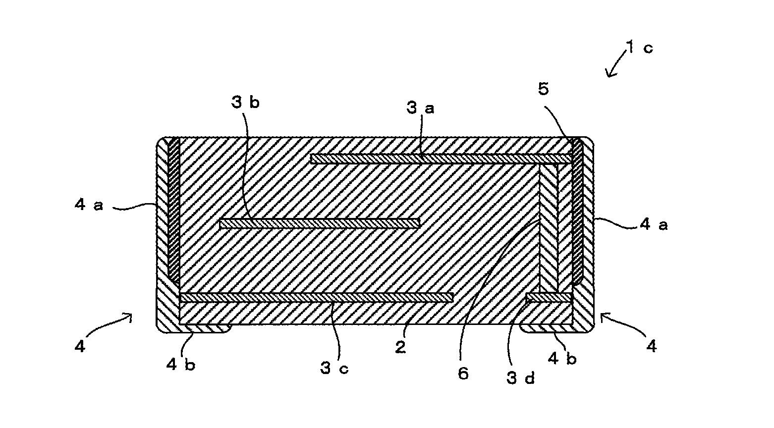
[0042]A chip-type electronic component 1c according to a third embodiment of the present disclosure will be described with reference to FIG. 4. Note that FIG. 4 is a cross-sectional view of the chip-type electronic component 1c.

[0043]The chip-type electronic component 1c according to the present embodiment differs from the chip-type electronic component 1a of the first embodiment having been discussed with reference to FIGS. 1 and 2 in a point that a part of each of the side surface electrodes 4 (corresponds to “second side-surface electrode” of the present disclosure) is formed on the cover layer 5 covering the side surface of the chip element assembly 2, as shown in FIG. 4. Because other constituent elements are the same as those of the chip-type electronic component 1a of the first embodiment, the same reference signs are assigned thereto and description thereof is omitted.

[0044]In this case, the cover layer 5 is formed by covering a portion of the side surface of the chip eleme...


PUM

PropertyMeasurementUnit
permittivityaaaaaaaaaa
dielectricaaaaaaaaaa
capacitanceaaaaaaaaaa

Abstract

A chip-type electronic component 1a mounted on a board includes a chip element assembly 2 having an upper surface, a lower surface, and a side surface; inner electrodes 3a, 3b, and 3c formed inside the chip element assembly 2; and a cover layer 5 that is formed with an insulation material having a lower permittivity than the chip element assembly 2 and is so provided as to cover at least part of the side surface of the chip element assembly 2. With this structure, unnecessary stray capacitance between the inner electrodes 3a, 3b, and 3c formed inside the chip element assembly 2 and other electrode members arranged outside the cover layer 5 in a direction orthogonal to a thickness direction of the chip element assembly 2 can be reduced, whereby the chip-type electronic component 1a capable of realizing the desired characteristics can be provided.

Description

[0001]This is a continuation of International Application No. PCT / JP2015 / 057999 filed on Mar. 18, 2015 which claims priority from Japanese Patent Application No. 2014-076309 filed on Apr. 2, 2014. The contents of these applications are incorporated herein by reference in their entireties.FIELD OF THE DISCLOSURE[0002]The present disclosure relates to chip-type electronic components each having an electrode formed inside a chip element assembly which is formed with dielectric material.DESCRIPTION OF THE RELATED ART[0003]Chip-type electronic components in which ceramic layers formed with different materials are laminated have been well-known. For example, as shown in FIG. 6, in a chip-type electronic component 100 disclosed in Patent Document 1, a chip element assembly 101 is formed in a laminated structure in which a high permittivity ceramic layer 101a having a relatively high permittivity and low permittivity ceramic layers 101b having a relatively low permittivity are laminated. In...

Claims


Application Information

Patent Timeline
Patent Type & Authority Applications(United States)
IPC IPC(8): H01G2/06H01G4/12H01G2/10H01G4/30H01G4/005H01G4/232
CPCH01G2/065H01G4/005H01G4/12H01G2/10H01G4/30H01G4/232
Inventor MATSUSHITA, YOSUKE
Owner MURATA MFG CO LTD
Why Eureka
Try Eureka