Stamp with structured posts

a post structure and post technology, applied in the field of stamps, can solve the problems of difficult to pick up and place ultra-thin, fragile or small devices using such conventional technologies, and many integrated circuits do not have a planar surface, so as to improve the reliability of the micro-transfer printing process, increase the adhesion force, and increase the contact surface height variation

Active Publication Date: 2017-02-16
X DISPLAY CO TECH LTD
View PDF6 Cites 47 Cited by
  • Summary
  • Abstract
  • Description
  • Claims
  • Application Information

AI Technical Summary

Benefits of technology

[0017]However, the distal end of a conventional post (i.e., the end of the post that is not attached to the body of the stamp) is typically a flat, planar surface orthogonal to the extension of the post. When applied to a micro-device that has a topographically structured surface and is therefore non-planar, the forces that adhere the micro-device to the distal end of the post are diminished because portions of the micro-device are not sufficiently close to the post. This reduction in contact adhesion can result in poor pick-up from the source wafer or loss of the micro-device during transport on the stamp post from the source wafer to the destination wafer. Although this problem is mitigated somewhat by the relatively soft and conformal post material, problems remain for micro-devices with substantially non-planar contact surfaces. A post 14 made of conformal material can be effective for micro-devices with a relatively smaller contact surface height variation but can fail for micro-devices with a relatively larger contact surface height variation. Similarly, a post 14 made of conformal material can be effective for micro-devices with a contact surface that is relatively planar but can fail for micro-devices with a contact surface that is relatively non-planar. Thus, the present invention enables micro-transfer printing of micro-devices having contact surfaces that have a greater contact surface height variation or are relatively non-planar.
[0018]According to an embodiment of the present invention, this problem is addressed with a stamp for micro-transfer printing that includes a body and one or more posts extending from the body, where at least one of the posts has a non-planar surface contour at the distal end of the post that has a size and shape that accommodates a non-planar contact surface of a micro-transfer printable device. By providing such a non-planar surface contour on the distal end of the post, the surface of the distal end of the post has a larger contact area with the micro-device than a planar surface thereby increasing the adhesion force between the surface of the distal end of the post and the non-planar contact surface of the micro-transfer printable device and improving the reliability of the micro-transfer printing process. The non-planar surface of the distal end of the post can substantially match, be geometrically similar to, or different from the non-planar contact surface of a micro-transfer printable device.
[0019]According to another embodiment of the present invention, a method of making a stamp with posts for micro-transfer printing includes providing a mold having a body portion and one or more post portions that extend away from the body portion, providing a device having a non-planar contact surface, filling the mold with curable stamp material and locating the non-planar contact surface of the device at the distal end of the post portion, and curing the curable stamp material to form a stamp for micro-transfer printing having a non-planar surface at the distal end of the post. The non-planar surface at the distal end of the post can be further processed to change the size or shape of any structures on the surface contour, for example to enhance the contact reliability.

Problems solved by technology

Conventional methods such as pick-and-place for applying integrated circuits to a destination substrate are limited to relatively large devices.
For example, having a dimension of a millimeter or more and it is often difficult to pick up and place ultra-thin, fragile, or small devices using such conventional technologies.
However, many integrated circuits do not have a planar surface whose area is readily contacted by a stamp post.

Method used


Image

  • Stamp with structured posts
  • Stamp with structured posts
  • Stamp with structured posts

Examples


Embodiment Construction

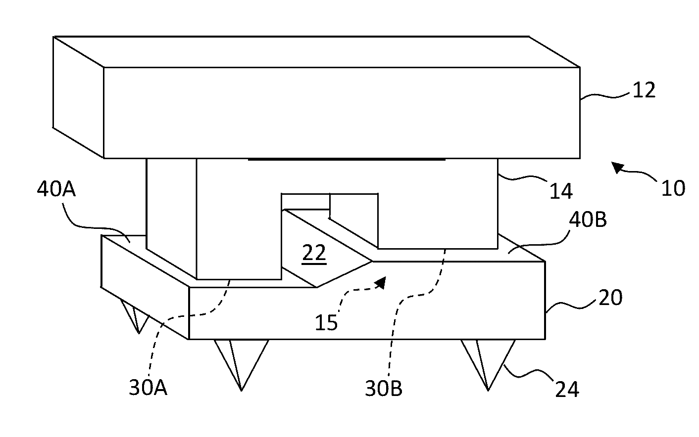
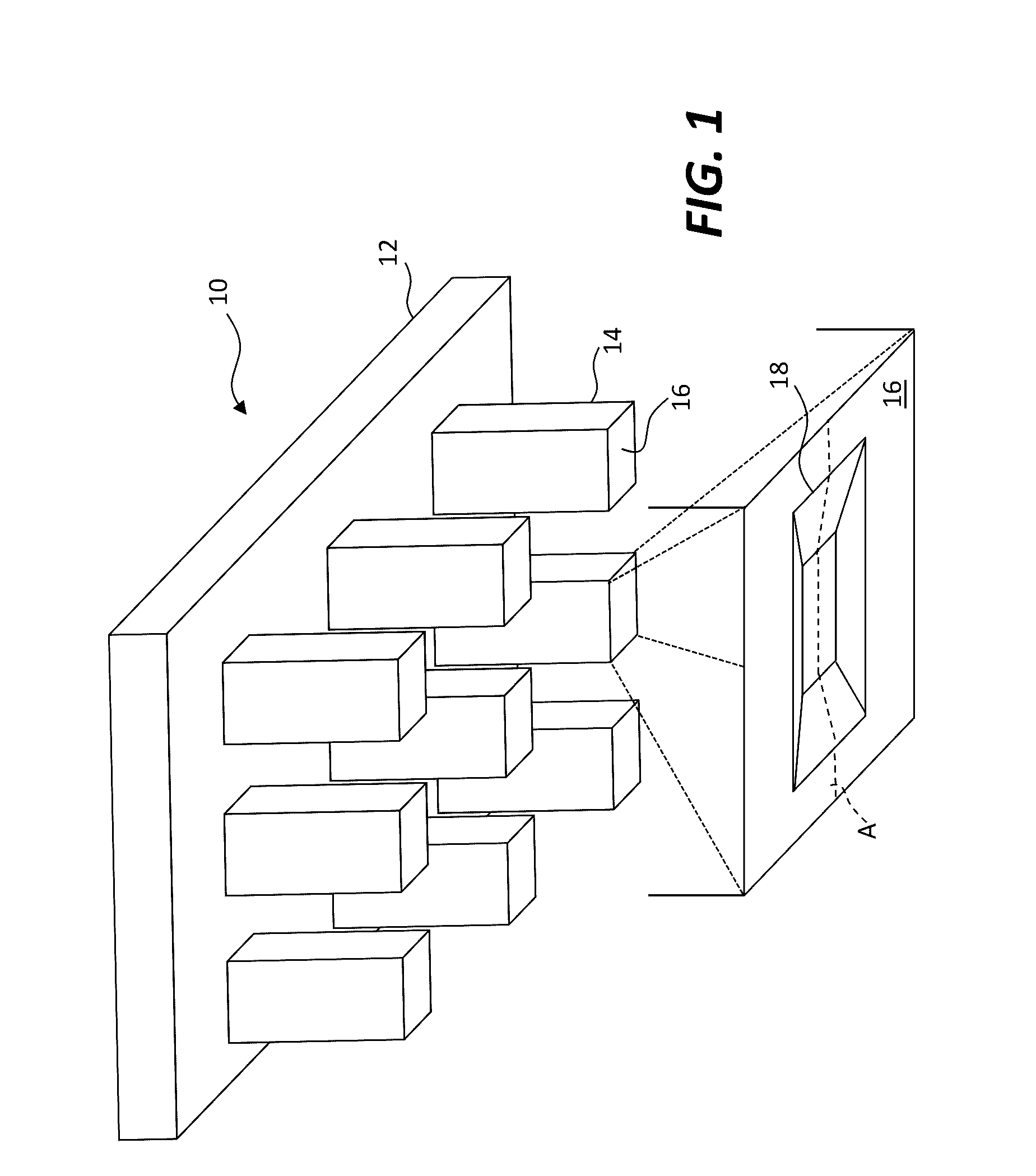
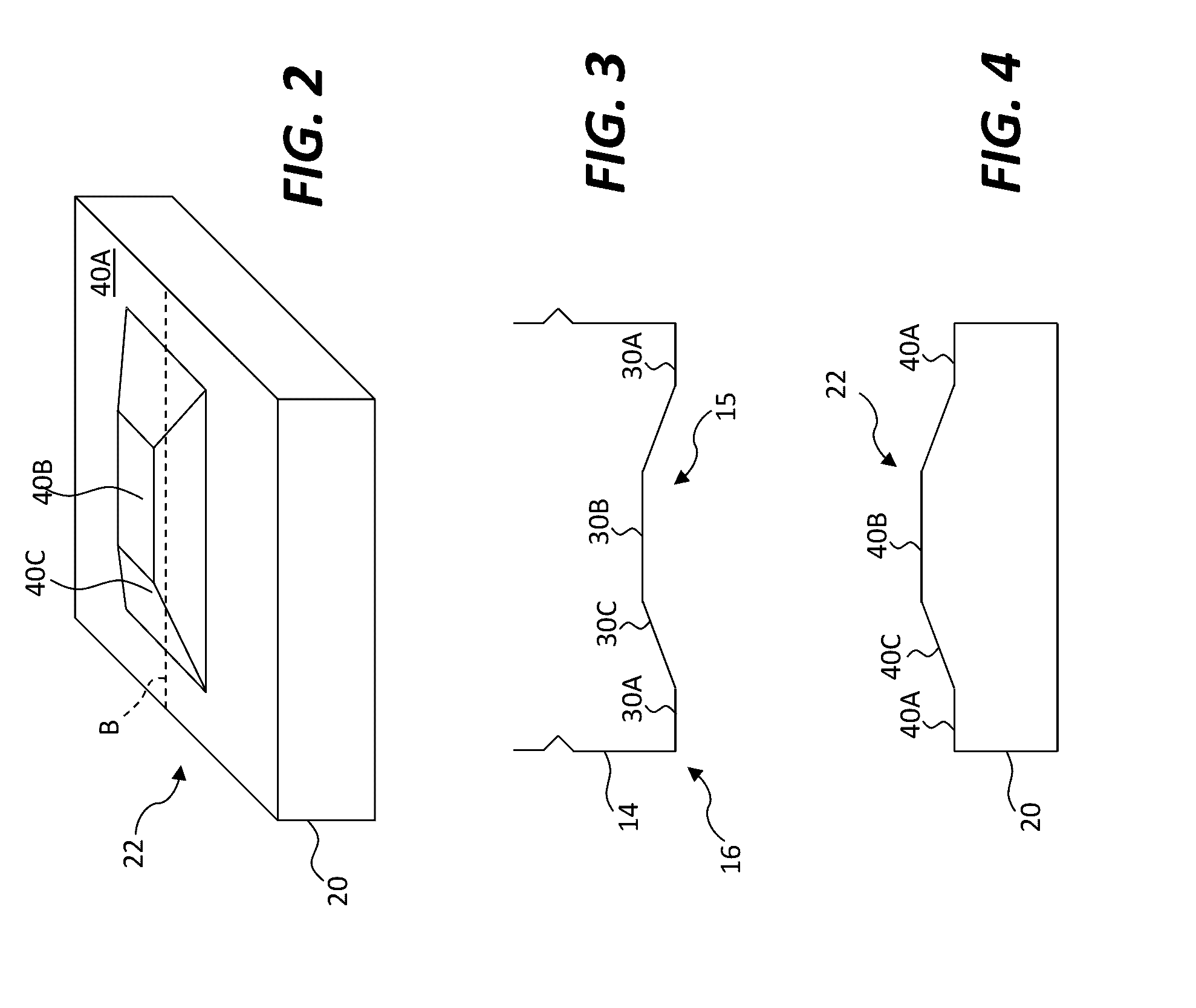
[0159]The present invention provides a stamp structure and methods of making and using the stamp for micro transfer printing micro-transfer printable devices. The micro-transfer printable devices can be light emitters or integrated circuits, for example CMOS integrated circuits made on or in a silicon semiconductor wafer, light-emitting diodes (LEDs), for example made on or in a GaN semiconductor material, or silicon photodiodes. The micro-transfer printable devices can have a width from 1-8 μm, a length from 5-10 μm, or a height from 0.5-3 μm. More generally, the micro-transfer printable devices can include or be a variety of chiplets having conductor or semiconductor structures, including a diode, a light-emitting diode (LED), a transistor, a laser, active electrical components, passive electrical components, or an electrical jumper.

[0160]Chiplets are small integrated circuits that can be unpackaged dies released from a source wafer and can be micro-transfer printed. Chiplets can ...


PUM

PropertyMeasurementUnit
heightaaaaaaaaaa
heightaaaaaaaaaa
diameteraaaaaaaaaa

Abstract

A stamp for micro-transfer printing includes a body and one or more posts extending from the body. At least one of the posts has a non-planar surface contour on the distal end of the post having a size, shape, or size and shape that accommodates a non-planar contact surface of a micro-transfer printable device.

Description

RELATED APPLICATIONS[0001]This application is a continuation-in-part of commonly assigned U.S. patent application Ser. No. 14 / 823,917 filed Aug. 11, 2015, entitled Printable Component Structure with Electrical Contact, which is hereby incorporated by reference in its entirety.FIELD OF THE INVENTION[0002]The present invention relates to stamps used in micro transfer printing.BACKGROUND OF THE INVENTION[0003]The disclosed technology relates generally to methods and tools for micro-transfer-printing. Conventional methods such as pick-and-place for applying integrated circuits to a destination substrate are limited to relatively large devices. For example, having a dimension of a millimeter or more and it is often difficult to pick up and place ultra-thin, fragile, or small devices using such conventional technologies. More recently, micro transfer printing methods have been developed that permit the selection and application of these ultra-thin, fragile, or small devices without causin...

Claims


Application Information

Patent Timeline
Patent Type & Authority Applications(United States)
IPC IPC(8): H01L23/00B29C59/00
CPCH01L24/81H01L24/75B29C59/002H01L2224/81345B41F16/00H01L2224/81986H01L2224/81901B29L2031/34H01L2224/81005B29C59/02B29C2059/023B29C2059/028B41F17/00H01L2224/75305H01L2224/75621H01L2224/81201H01L2224/13013H01L2224/13016H01L21/7806H01L25/0753H01L33/0095H01L2224/16227H01L2924/00014H01L33/0093H01L2224/13099H01L21/6835H01L24/95B29C33/3842B29C59/026B29L2007/001
Inventor MEITL, MATTHEWBOWER, CHRISTOPHERCOK, RONALD S.
Owner X DISPLAY CO TECH LTD
Why Eureka
Try Eureka