Pixel circuit and organic light emitting display device having the same

a display device and circuit technology, applied in semiconductor devices, instruments, electrical devices, etc., can solve the problems of inability to perform real-time pixel current sensing operations, light blur, and typical pixel structures, so as to reduce display quality may be maintained, and the effect of reducing the sensing time for compensating image data

a display device and circuit technology, applied in semiconductor devices, instruments, electrical devices, etc., can solve the problems of inability to perform real-time pixel current sensing operations, light blur, and typical pixel structures, so as to reduce display quality may be maintained, and the effect of reducing the sensing time for compensating image data

US20170061877A1Active Publication Date: 2017-03-02SAMSUNG DISPLAY CO LTD

Image

  • Pixel circuit and organic light emitting display device having the same
  • Pixel circuit and organic light emitting display device having the same
  • Pixel circuit and organic light emitting display device having the same

Examples


Embodiment Construction

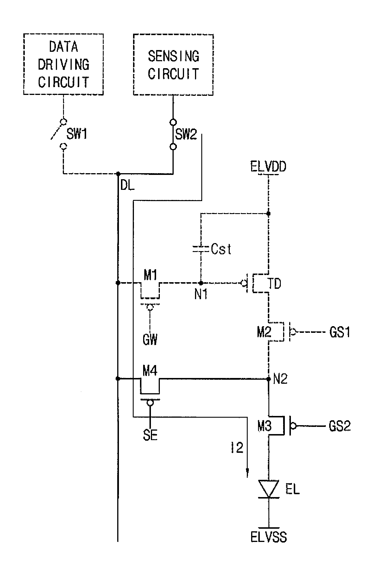
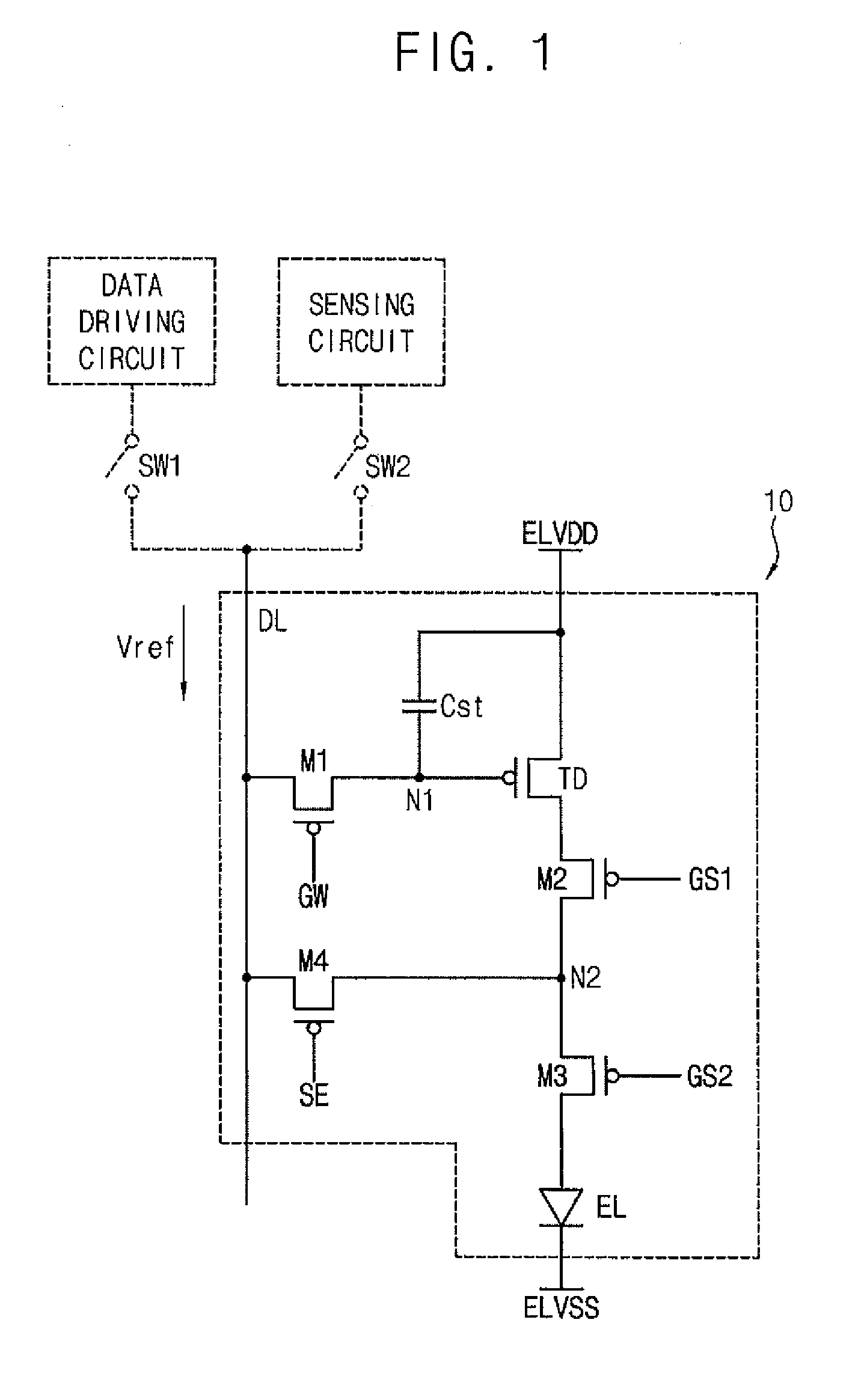
[0043]Exemplary embodiments will be described more fully hereinafter with reference to the accompanying drawings, in which various embodiments are shown.

[0044]It will be understood that, although the terms “first”, “second”, “third”, etc., may be used herein to describe various elements, components, regions, layers, and / or sections, these elements, components, regions, layers and / or sections should not be limited by these terms. These terms are used to distinguish one element, component, region, layer or section from another element, component, region, layer or section. Thus, a first element, component, region, layer, or section discussed below could be termed a second element, component, region, layer, or section, without departing from the spirit and scope of the present invention.

[0045]Further, it will also be understood that when one element, component, region, layer and / or section is referred to as being “between” two elements, components, regions, layers, and / or sections, it c...


PUM


Abstract

A pixel circuit according to example embodiments includes a scan switch connected between a data line and a first node, a storage capacitor, an organic light emitting diode, a driving transistor connected to a first power voltage and configured to generate a driving current, a first control switch connected between the driving transistor and a second node and configured to be turned on during a first sensing period based on a first control signal, a second control switch connected between the second node and an anode of the organic light emitting diode and configured to be turned on during a second sensing period based on a second control signal, and a sensing switch connected between the data line and the second node and configured to be turned on based on a sensing control signal.

Description

CROSS REFERENCE TO RELATED APPLICATION[0001]This application claims priority to and the benefit of Korean Patent Applications No. 10-2015-0118654, filed on Aug. 24, 2015 in the Korean Intellectual Property Office (KIPO), the disclosure of which is hereby incorporated by reference herein in its entirety.BACKGROUND[0002]1. Field[0003]Example embodiments of the inventive concept relate to display devices and to organic light emitting display devices including organic light emitting diodes.[0004]2. Description of the Related Art[0005]An organic light emitting display device displays images using organic light emitting diodes. Because degradation of the organic light emitting diodes and a difference in the threshold voltage / mobility of a driving transistor may occur, luminance variations and image blur may be noticeable.[0006]Typical organic light emitting display devices detect a pixel current and calculate a degradation of a pixel based on the detected pixel current. However, typical p...

Claims


Application Information

Patent Timeline
02 Mar 2017
Publication
US20170061877A1
IPC
G09G3/3233; G09G3/20; G09G3/3258; H01L27/32
CPC
G09G3/3233; H01L27/3276; H01L27/3265; H01L27/3262; G09G2330/04; G09G3/3258; G09G2300/0426; G09G2310/0251
Inventors
LEE, GIL-JAE