Method of forming bit line of flash memory device

a flash memory device and bit line technology, applied in the field of fabricating semiconductor devices, can solve the problems of increasing the resistance shrinking the space between the first metal lines m-b>1/b>, increasing the sensing time, etc., and reducing the sensing time, preventing the increase of the capacitance of the bit line, and minimizing the distance between the bit lines

Active Publication Date: 2006-11-30
SK HYNIX INC
View PDF4 Cites 13 Cited by
  • Summary
  • Abstract
  • Description
  • Claims
  • Application Information

AI Technical Summary

Benefits of technology

[0012] An embodiment of the present invention provides a method of forming bit lines of a flash memory device, wherein an increase in the capacitance of the bit lines can be prevented and the distance between the bit lines can also be minimized, thereby reducing the sensing time.

Problems solved by technology

This reduction in pattern size can lead to crosstalk.
However, if the pitch of the metal line is reduced to obtain a higher capacity of the device, the space between the first metal lines M-1 also shrinks.
However, if the thickness (W) of the bit line and the distance (S) between the bit lines are excessively reduced, the resistance of the bit line increases.
Accordingly, there is a problem with increasing sensing time since the capacitance between the bit lines increases.

Method used


Image

  • Method of forming bit line of flash memory device
  • Method of forming bit line of flash memory device
  • Method of forming bit line of flash memory device

Examples


Embodiment Construction

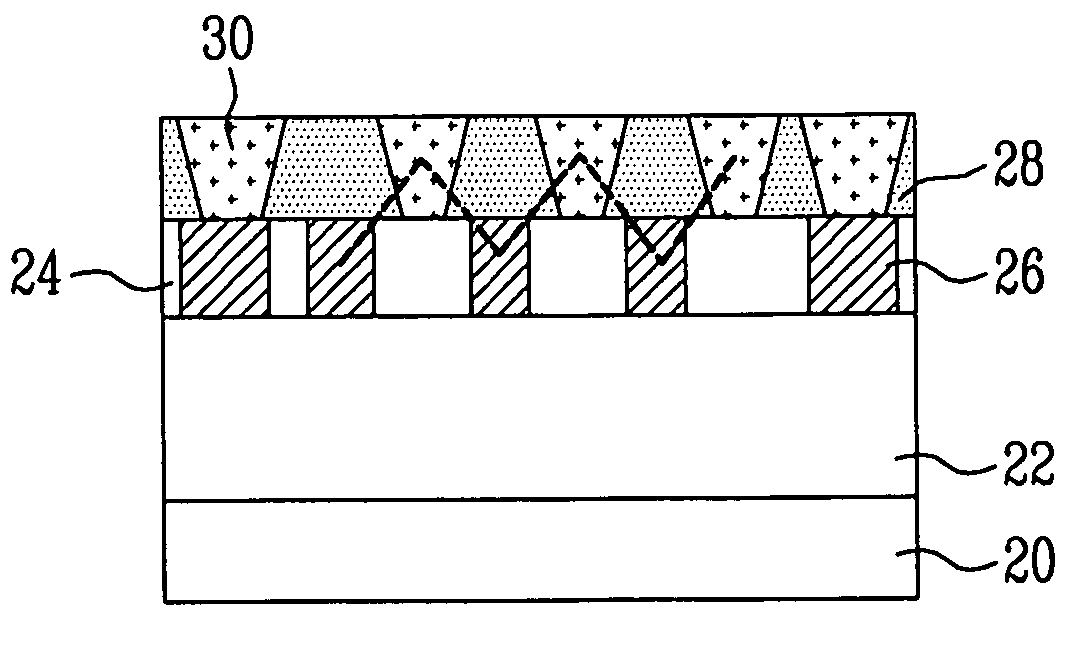
[0030] In the following detailed description, only certain embodiments of the present invention have been shown and described simply by way of illustration. As those skilled in the art will realize, the described embodiments may be modified in various ways, all without departing from the spirit or scope of the present invention. When it is said that any part, such as a layer, film, area, or plate, is positioned on another part, it means the part is directly on the other part or above the other part with at least one intermediate part. On the other hand, if any part is said to be positioned directly on another part it means that there is no intermediate part between the two parts.

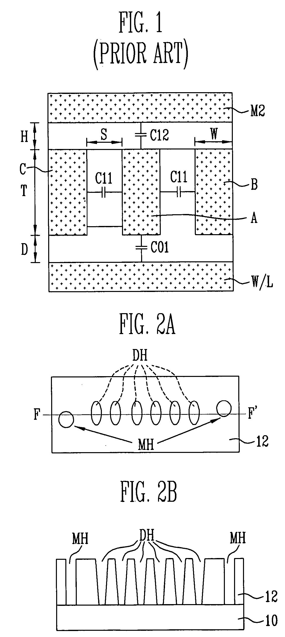
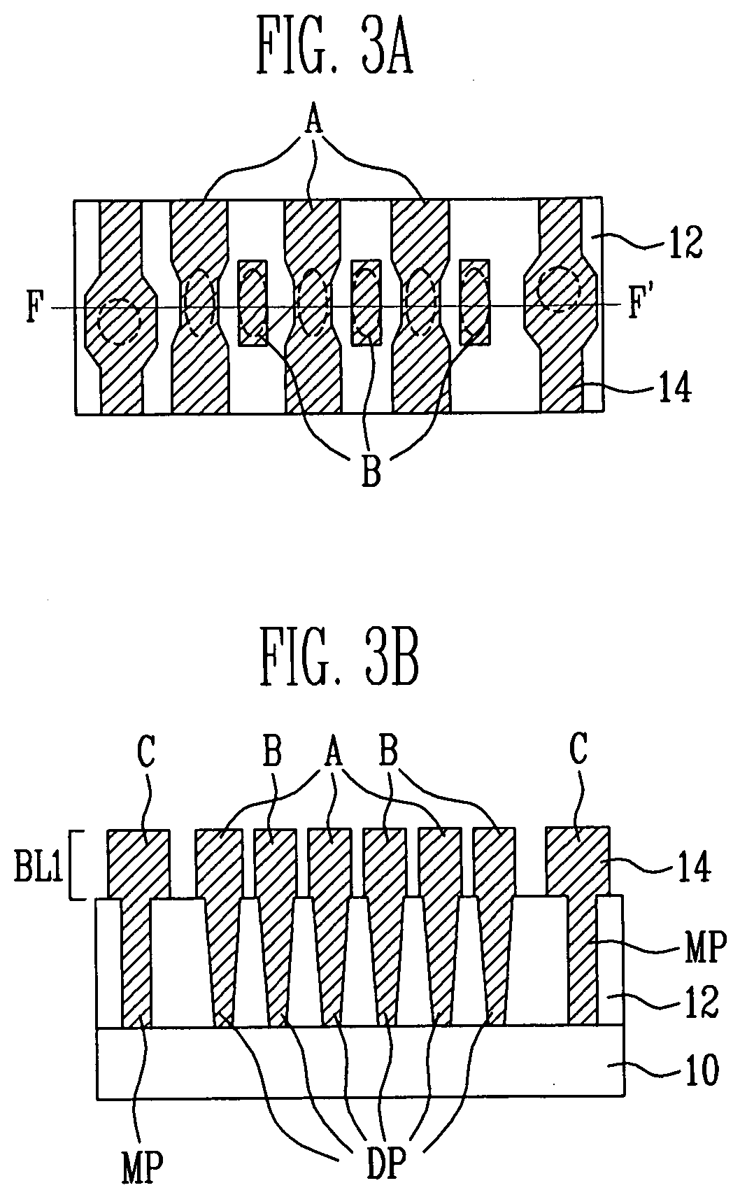
[0031]FIGS. 2A, 2B, 3A, 3B, 4A, 4B, 5A, 5B and 5C are cross-sectional views and layout diagrams illustrating a method of forming bit lines of a flash memory device according to a first embodiment of the present invention. FIGS. 2A, 3A, 4A, and 5A are layout diagrams illustrating the method of forming the bi...


PUM


Abstract

A method for forming a semiconductor device includes forming a plurality of drain contact holes in a first interlayer insulating layer provided over a semiconductor substrate. First metal material having a predetermined thickness is formed over the first interlayer insulating layer, the first metal material filling the drain contact holes. A first metal layer is formed by patterning the first metal material, the first metal layer having a plurality of lines of a first type and a plurality of landing pads. A second interlayer insulating layer is formed over the patterned first metal material. A plurality of trenches is formed in the second interlayer insulating layer, the trenches exposing the landing pads. A second metal layer is formed by providing second metal material over the second interlayer insulating layer and filling the trenches, the second metal layer including a plurality of lines of a second type defined within the trenches, the lines of the second type contacting the landing pads. The first and second metal layers define a first metal level of the semiconductor device. The lines of the first type define odd-number lines of the first metal level, and the lines of the second type define even-number lines of the first metal level.

Description

BACKGROUND [0001] The present invention relates to a method of fabricating semiconductor devices, and more particularly, to a method of forming bit lines of a flash memory device. [0002] In flash memory devices, the pattern size of lower elements is continuously being reduced. This reduction in pattern size can lead to crosstalk. To reduce the crosstalk problem, the space width of the oxide film is maximized. However, if the pitch of the metal line is reduced to obtain a higher capacity of the device, the space between the first metal lines M-1 also shrinks. [0003]FIG. 1 is a cross-sectional view illustrating the problem with a reduction in pattern size between the bit lines of the flash memory device in the related art. [0004] Referring to FIG. 1, metal films that generate the coupling capacitor adjacent to the bit line A include a lower word line W / L, bit lines B, C parallel to the bit line A, an upper metal line M2, and so on. The word line W / L and the bit line A are separated by...

Claims


Application Information

Patent Timeline
Patent Type & Authority Applications(United States)
IPC IPC(8): H01L21/4763
CPCH01L21/76804H01L21/76816H01L27/11521H01L21/76895H01L27/115H01L21/76838H10B69/00H10B41/30H01L23/5283H01L21/76885H01L21/76897
Inventor JUNG, WOO YUNGKIM, TAE KYUNGKIM, EUN SOO
Owner SK HYNIX INC
Why Eureka
Try Eureka