Semiconductor memory device with reduced sense amplification time and operation method thereof

Inactive Publication Date: 2008-10-02
SK HYNIX INC
View PDF22 Cites 12 Cited by
  • Summary
  • Abstract
  • Description
  • Claims
  • Application Information

AI Technical Summary

Benefits of technology

[0019]Embodiments of the present invention are directed to providing a semiconductor memory device capabl

Problems solved by technology

On the other hand, the read operation of the semiconductor memory device becomes slow if the time of ‘

Method used


Image

  • Semiconductor memory device with reduced sense amplification time and operation method thereof
  • Semiconductor memory device with reduced sense amplification time and operation method thereof
  • Semiconductor memory device with reduced sense amplification time and operation method thereof

Examples


Example

[0032]Hereinafter, a semiconductor memory device in accordance with the present invention will be described in detail referring to the accompanying drawings.

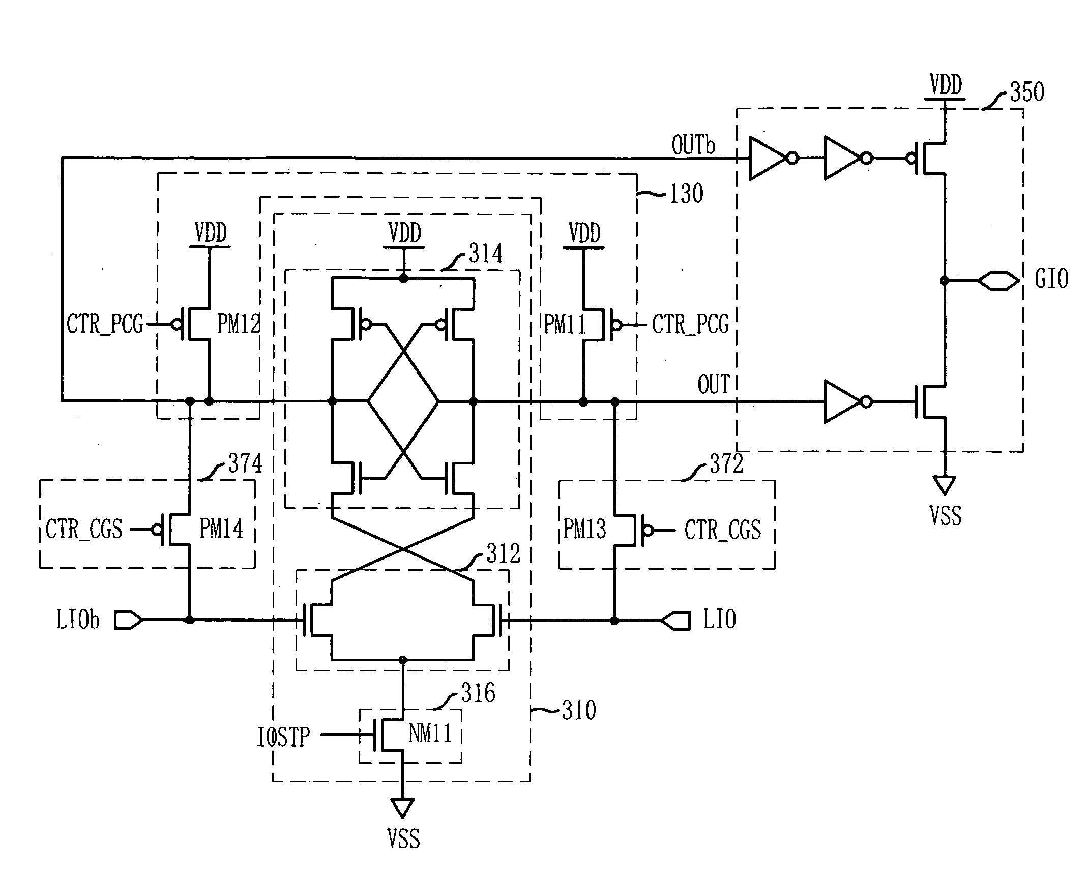
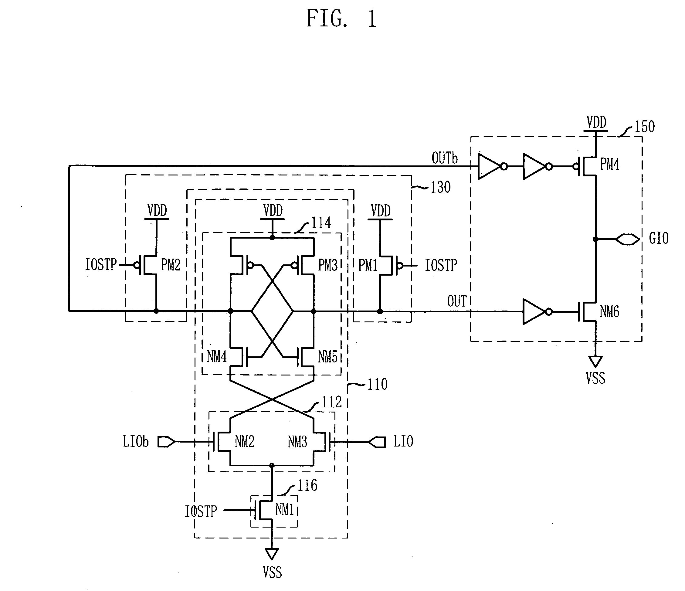
[0033]FIG. 3 is a circuit diagram illustrating an I / O sense amplifier according to the present invention. A sense amplifying unit 310 senses and amplifies data, which are applied to positive and negative local I / O lines LIO and LIOb, in response to an I / O strobe signal IOSTP. A precharging unit 330 precharges the output terminals OUT and OUTb of the sense amplifying unit 310 in response to a precharge signal CTR_PCG. A charge sharing unit (including charge sharing elements 372 and 374) cause a charge sharing between the first and second output terminals OUT and OUTb and the corresponding positive / negative local I / O lines LIO and LIOb, before the sensing and amplifying section of the sense amplifying unit 310. A pull-up / pull-down driving unit 350 pull-up / pull-down drives the global I / O line GIO in response to an output signal of ...


PUM


Abstract

A semiconductor memory device is capable of swiftly sensing data loaded on local I/O lines and transferring the sensed data to a global I/O line, thereby reducing an operating time of a sense amplifier by increasing the sensing and amplifying speed. The semiconductor memory device includes a sense amplifying unit, a precharging unit, a charge sharing unit, and a driving unit. The sense amplifying unit amplifies data applied to a first data line in response to an I/O strobe signal. The precharging unit precharges an output unit of the sense amplifying unit in response to a precharge signal. The charge sharing unit performs a charge sharing operation between the first data line and the output unit before a sense amplifying operation of the sense amplifying unit. The driving unit drives a second data line in response to an output signal of the sense amplifying unit.

Description

CROSS-REFERENCE TO RELATED APPLICATIONS[0001]The present invention claims priority to Korean patent application number. 10-2007-0032536, filed on Apr. 2, 2007, which is incorporated by reference in its entirety.BACKGROUND OF THE INVENTION[0002]The present invention relates to a semiconductor design technology, and more particularly to a semiconductor memory device capable of rapidly transferring data, which are applied to local I / O lines, to a global I / O line.[0003]A plurality of memory banks are provided within a semiconductor memory device such as a DDR SDRAM (Double Data Rate Synchronous DRAM) and each memory bank is comprised of a set of a plurality of memory cells each of which has a cell transistor and a cell capacitor. Herein, an area in which the memory bank is positioned is called “core area” and an area to input and output the data to and from the memory bank is called “peripheral area.” The data transferred from the peripheral area at a write operation are inputted into t...

Claims


Application Information

Patent Timeline
IPC IPC(8): G11C7/08G11C7/06
CPCG11C7/08G11C11/4091G11C7/1048G11C7/222G11C11/4096
Inventor DO, CHANG-HO
Owner SK HYNIX INC
Why Eureka
Try Eureka