Method for manufacturing multilayer substrate

a technology of multi-layer substrates and manufacturing methods, applied in the direction of dielectric characteristics, insulation conductors/cables, thermoplastic polymer dielectrics, etc., can solve the problems of time and effort, and achieve the effect of easy formation of inter-layer connection conductors

Inactive Publication Date: 2017-03-02
MURATA MFG CO LTD
View PDF0 Cites 1 Cited by
  • Summary
  • Abstract
  • Description
  • Claims
  • Application Information

AI Technical Summary

Benefits of technology

[0006]Preferred embodiments of the present invention provide a method for manufacturing a multilayer substrate, the method being capable of easily forming an interlayer connection conductor on a multilayer substrate.
[0008]In this configuration, by forming the penetrating hole that penetrates the interlayer connection conductor in the laminating direction, the penetrating hole (through hole) is able to be formed so that the interlayer connection conductor may be exposed to the inner wall of the through hole. This forms a through hole of which the inner wall is provided with an interlayer connection conductor. Therefore, since it is not necessary to perform electroless plating and a pretreatment of the electroless plating in order to form the through hole of which the inner wall is provided with the interlayer connection conductor, a through hole of which the inner wall is provided with the interlayer connection conductor is able to be formed easily.
[0009]A method for manufacturing a multilayer substrate according to a preferred embodiment of the present invention may further preferably include a step of growing a metal film on the interlayer connection conductor exposed to an inner side of a penetrated portion of the region. In this configuration, since the layers of the multilayer substrate is connected by a metal film of which the conductor resistance is small compared with the interlayer connection conductor, power loss in an interlayer connection portion is significantly reduced.
[0011]In a method for manufacturing a multilayer substrate according to a preferred embodiment of the present invention, the base material may preferably include a main surface on which conductive foil is formed; and the conductive foil may preferably include a first main surface that is in contact with the base material; and a second main surface that is not in contact with the base material, and surface roughness of the first main surface may preferably be larger than surface roughness of the second main surface. In this configuration, it is possible to ensure the joining strength of the conductive foil and the insulating layer and to prevent the conductor resistance from deteriorating.
[0012]In a method for manufacturing a multilayer substrate according to a preferred embodiment of the present invention, the base material may preferably include a main surface on which metal foil is formed; and in the step of stacking and integrating the plurality of the base materials, first metal included in the metal foil and second metal included in the interlayer connection conductor may preferably form a solid phase diffusion layer between the metal foil and the interlayer connection conductor. In this configuration, the metal foil and the interlayer connection conductor are joined by metallic bonding, which increases the joining strength between the metal foil and the interlayer connection conductor.
[0014]According to various preferred embodiments of the present invention, it is possible to easily form an interlayer connection conductor on a multilayer substrate.

Problems solved by technology

Therefore, the method disclosed in Japanese Unexamined Patent Application Publication No. 2006-012895 requires time and effort when forming a conductive layer in a penetrating hole.

Method used


Image

  • Method for manufacturing multilayer substrate
  • Method for manufacturing multilayer substrate
  • Method for manufacturing multilayer substrate

Examples


Embodiment Construction

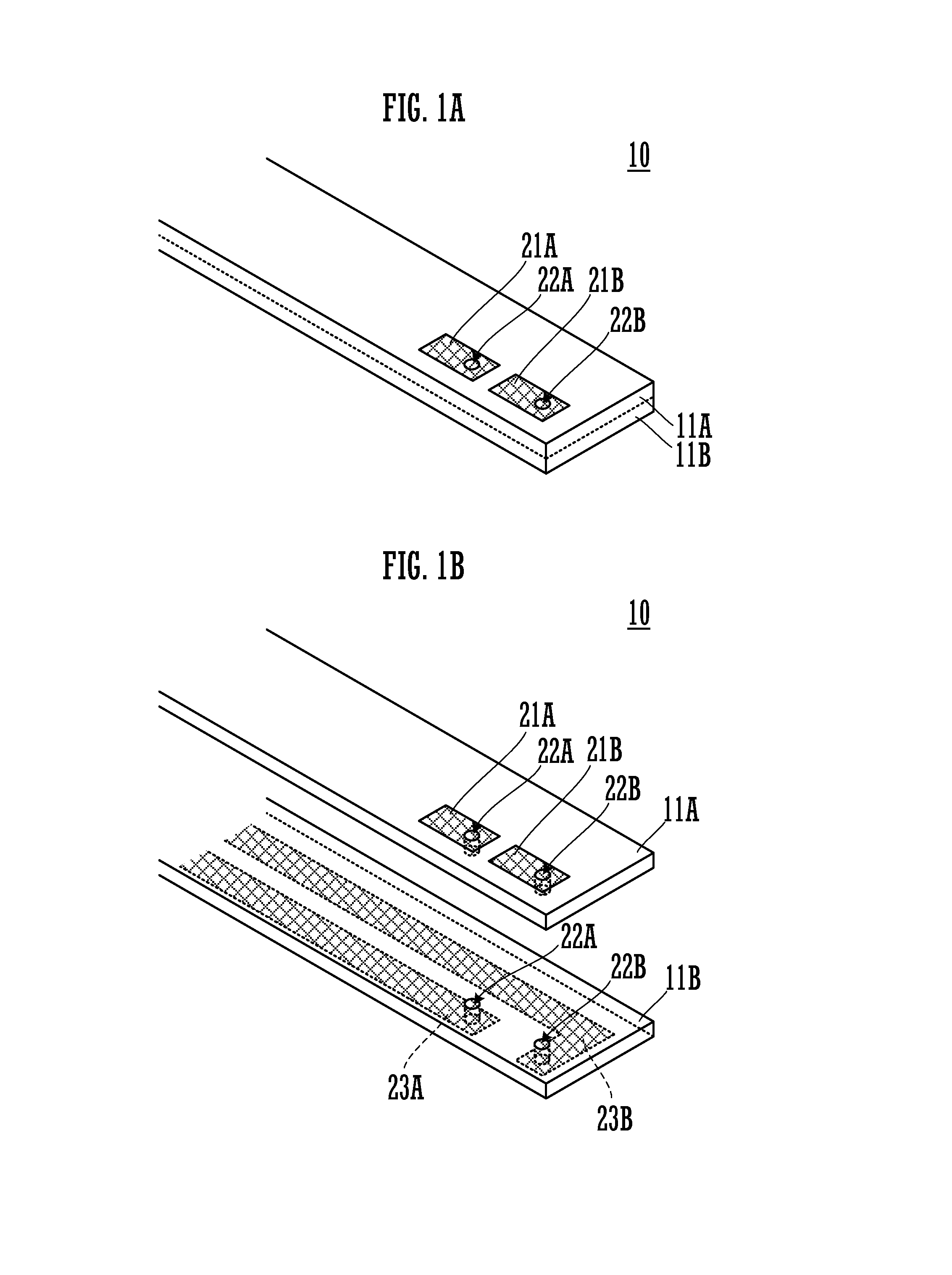
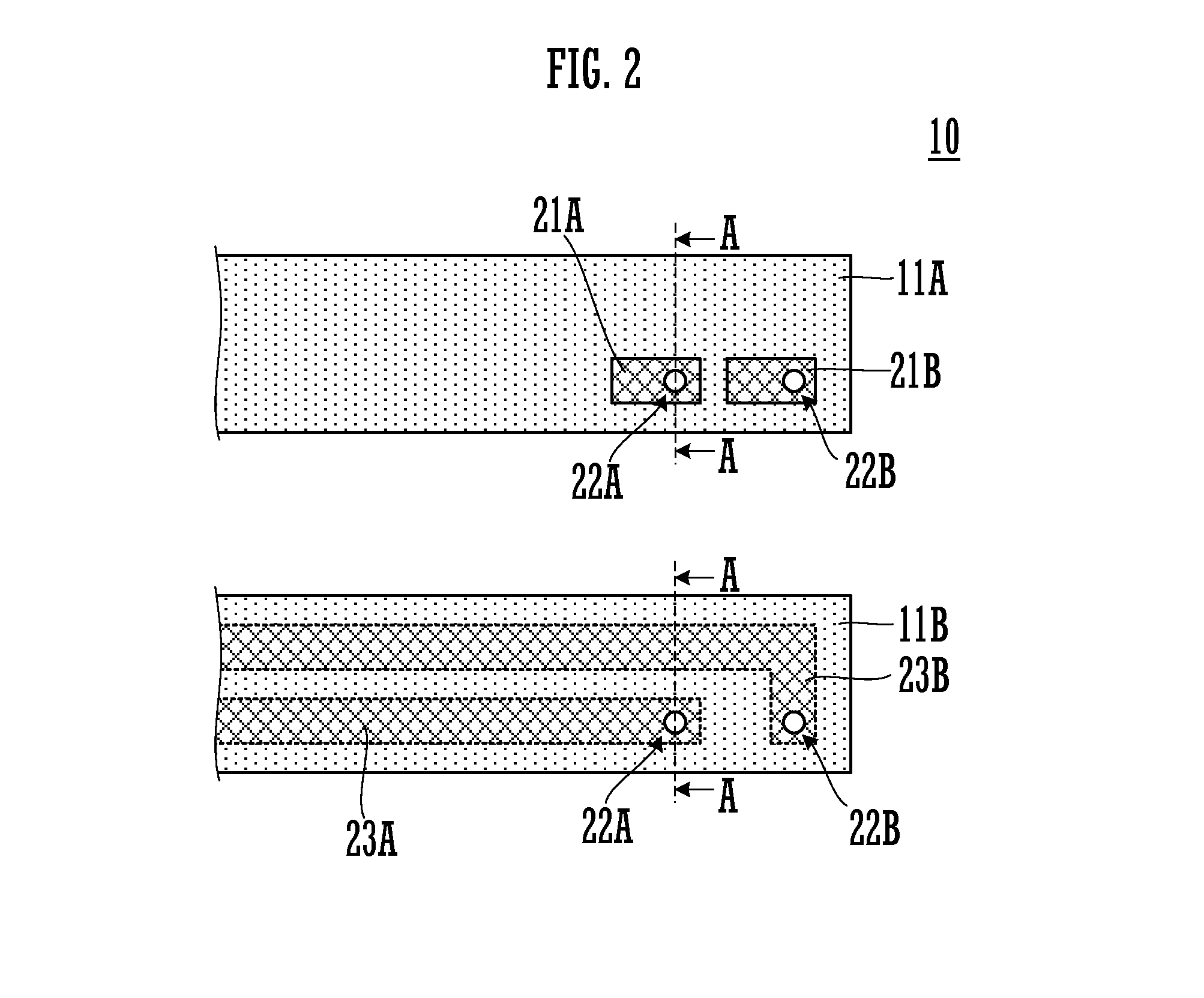
[0028]Hereinafter, a flexible cable 10 according to a preferred embodiment of the present invention will be described. The flexible cable 10 is an example of a multilayer substrate of the present invention. FIG. 1A is an external perspective view showing a vicinity of an end portion of the flexible cable 10. FIG. 1B is an exploded perspective view showing the vicinity of the end portion of the flexible cable 10. FIG. 2 is an exploded plan view showing the vicinity of the end portion of the flexible cable 10.

[0029]The flexible cable 10 preferably has a rectangular or substantially rectangular plate-shaped configuration and extends in the longitudinal direction. The flexible cable 10 includes an insulating layer (base material) 11A and an insulating layer 11B that are laminated on each other. In the flexible cable 10, the insulating layer 11A is stacked on the upper surface of the insulating layer 11B. The flexible cable 10 includes an external electrode 21A and an external electrode ...


PUM

PropertyMeasurementUnit
conductiveaaaaaaaaaa
surface roughnessaaaaaaaaaa
flexibleaaaaaaaaaa

Abstract

In a method for manufacturing a multilayer substrate, first, a via hole is formed in a first insulating layer and a second insulating layer and filled with conductive paste. Subsequently, the first insulating layer and the second insulating layer are stacked on each other. Next, the conductive paste is cured to form a via conductor while the first insulating layer and the second insulating layer are integrated through thermal pressing. Then, a penetrating hole that penetrates the via conductor in the laminating direction is formed.

Description

BACKGROUND OF THE INVENTION[0001]1. Field of the Invention[0002]The present invention relates to a method for manufacturing multilayer substrates including interlayer connection conductors.[0003]2. Description of the Related Art[0004]In some conventional multilayer substrates, layers may have been connected by a metal film that forms an inner wall of a through hole. As a method for manufacturing a through hole that connects the upper surface and the lower surface of a substrate, for example, Japanese Unexamined Patent Application Publication No. 2006-012895 discloses a method for manufacturing a semiconductor device. In the method for manufacturing a semiconductor device, an inorganic insulating layer is formed on the inner wall of a penetrating hole of a semiconductor substrate to form an organic insulating layer on the inorganic insulating layer via an adhesion promoting layer. Then, on the organic insulating layer, a conductive layer that connects the upper surface side and the l...

Claims


Application Information

Patent Timeline
Patent Type & Authority Applications(United States)
IPC IPC(8): H01B13/00H01B13/06
CPCH01B13/0036H01B13/06H01B13/0016H01L21/486H01L23/49822H01L23/49827H05K1/115H05K3/246H05K3/363H05K3/4069H05K3/4632H05K2201/0129H05K2201/0154H05K2201/09181H05K2201/09527H05K2201/09572
Inventor YOSUI, KUNIAKI
Owner MURATA MFG CO LTD
Why Eureka
Try Eureka