Lateral-Diode, Vertical-SCR Hybrid Structure for High-Level ESD Protection

Active Publication Date: 2017-03-09
HONG KONG APPLIED SCI & TECH RES INST
View PDF11 Cites 18 Cited by
  • Summary
  • Abstract
  • Description
  • Claims
  • Application Information

AI Technical Summary

Problems solved by technology

Integrated circuits (IC's) are prone to damage and failure from an electro-static-discharge (ESD) pulse.
ESD failures may occur in the factory and contribute to lower yields.
ESD failures may also occur in the field when an end-user touches a device.
Smaller devices such as security chips in a smart credit-card or bank card are especially prone to ESD failure.
As credit cards are replaced with smart cards using Integrated Circuit (IC) chips, many ESD failures will occur using the present ESD technology.
These smaller transistors are much more susceptible to over-voltage failure but can operate with a lower power-supply voltage, thus consuming less power and producing less heat.
Static charges from a person or machinery can produce such damaging currents that are only partially blocked by the input-protection circuits in the periphery.
Some prior-art ESD protecti

Method used


Image

  • Lateral-Diode, Vertical-SCR Hybrid Structure for High-Level ESD Protection
  • Lateral-Diode, Vertical-SCR Hybrid Structure for High-Level ESD Protection
  • Lateral-Diode, Vertical-SCR Hybrid Structure for High-Level ESD Protection

Examples


Embodiment Construction

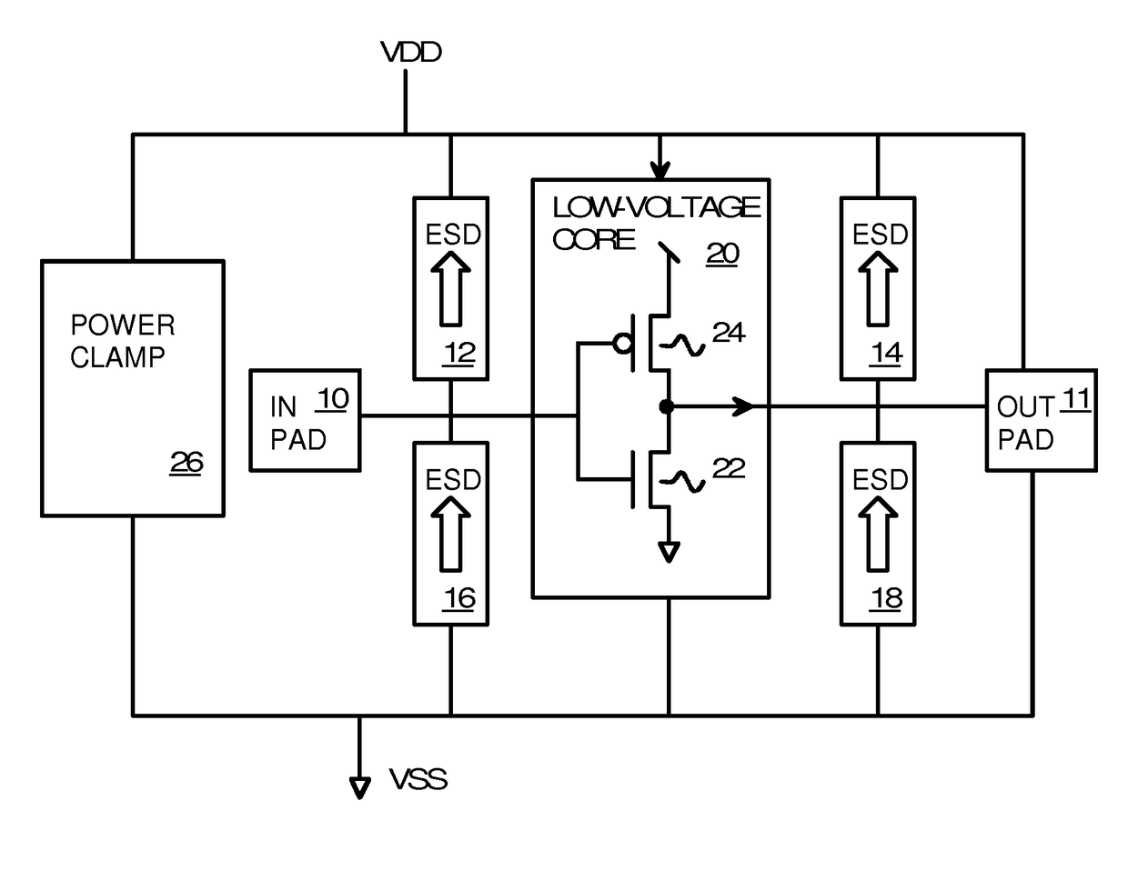
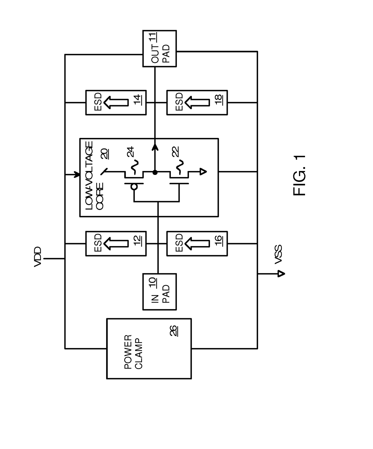
[0029]The present invention relates to an improvement in ESD protection circuits. The following description is presented to enable one of ordinary skill in the art to make and use the invention as provided in the context of a particular application and its requirements. Various modifications to the preferred embodiment will be apparent to those with skill in the art, and the general principles defined herein may be applied to other embodiments. Therefore, the present invention is not intended to be limited to the particular embodiments shown and described, but is to be accorded the widest scope consistent with the principles and novel features herein disclosed.

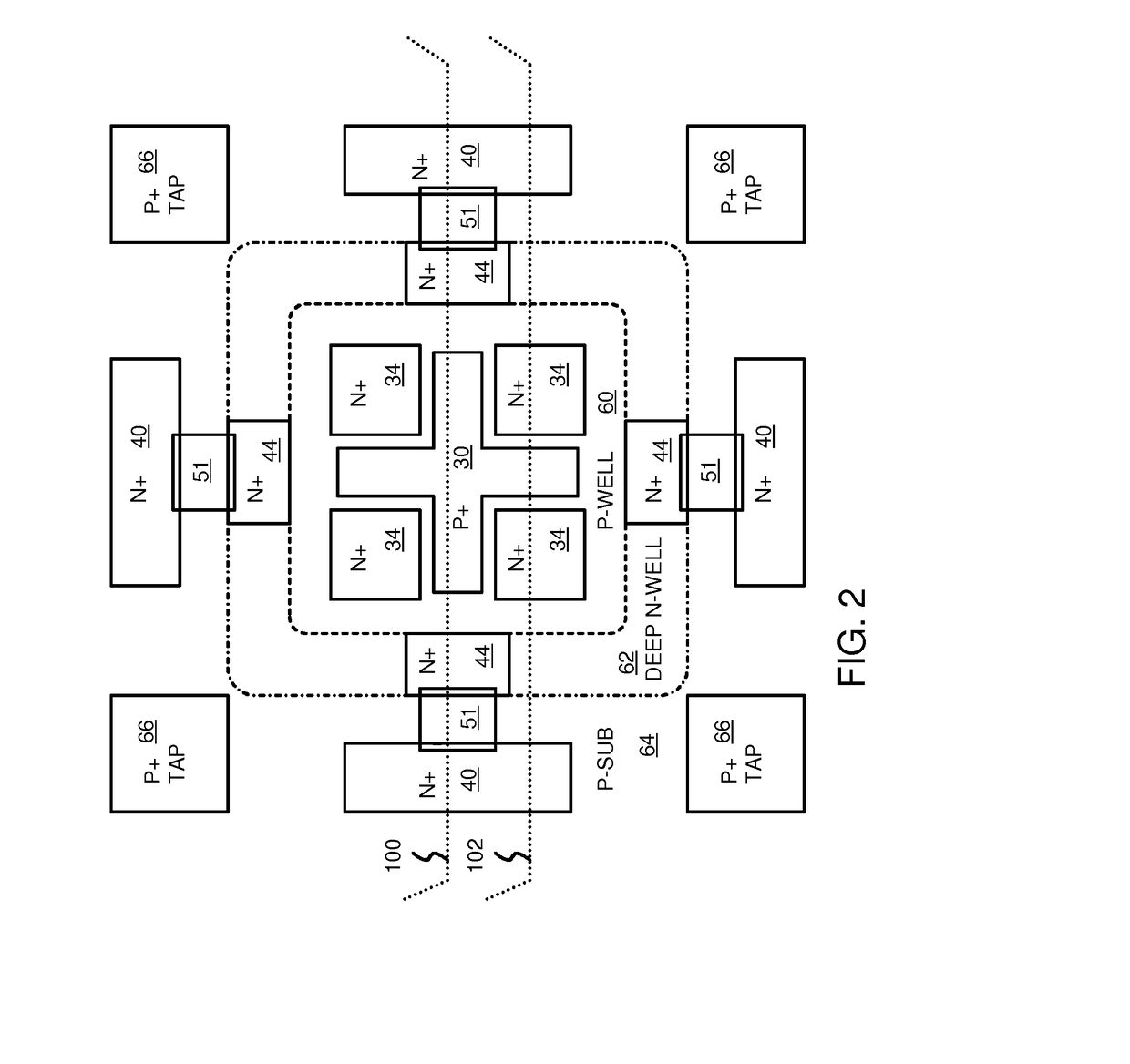
[0030]The inventors realize that an ESD-protection device having both an SCR and a diode can be constructed by tightly integrating the diode into the SCR structure. In particular, the inventors realize that the diode may be placed in the middle of the SCR layout. A lateral diode may be placed at the center of a square or ring-...


PUM


Abstract

A lateral p-n diode in the center of and surrounded by a vertical Silicon-Controlled Rectifier (SCR) forms an Electro-Static-Discharge (ESD) protection structure. The lateral p-n diode has a cross-shaped P+ diode tap with four rectangles of N+ diode regions in each corner of the cross. A P-well under the P+ diode tap is also an anode of a vertical PNPN SCR that has a deep N-well in a P-substrate. The deep N-well surrounds the lateral diode. Triggering MOS transistors are formed just beyond the four ends of the cross shaped P+ diode tap. Each triggering MOS transistor has N+ regions at the edge of the deep N-well and in the P-substrate that act as the cathode terminals. A deep P+ implant region under the N+ region at the edge of the deep N-well decreases a trigger voltage of the vertical SCR.

Description

FIELD OF THE INVENTION[0001]This invention relates to electro-static-discharge (ESD) protection circuits, and more particularly to Silicon-Controlled Rectifier (SCR) structures that have ESD-protection diodes integrated within them.BACKGROUND OF THE INVENTION[0002]Integrated circuits (IC's) are prone to damage and failure from an electro-static-discharge (ESD) pulse. ESD failures may occur in the factory and contribute to lower yields. ESD failures may also occur in the field when an end-user touches a device. Smaller devices such as security chips in a smart credit-card or bank card are especially prone to ESD failure. As credit cards are replaced with smart cards using Integrated Circuit (IC) chips, many ESD failures will occur using the present ESD technology.[0003]Various ESD-protection structures have been placed near input, output, or bi-directional I / O pins of ICs. Many of these protection structures use passive components such as series resistors, diodes, and thick-oxide tra...

Claims


Application Information

Patent Timeline
IPC IPC(8): H01L27/02H01L29/749H01L29/74
CPCH01L27/0255H01L29/749H01L29/7412H01L27/0262H01L29/861H01L29/0692
Inventor CAI, XIAOWUYAN, BEIPINGCHEN, ZHONGZI
Owner HONG KONG APPLIED SCI & TECH RES INST
Why Eureka
Try Eureka