Semiconductor device having supporters and method of manufacturing the same

Active Publication Date: 2017-03-16
SAMSUNG ELECTRONICS CO LTD
View PDF3 Cites 17 Cited by
  • Summary
  • Abstract
  • Description
  • Claims
  • Application Information

AI Technical Summary

Benefits of technology

[0007]Some example embodiments of the inventive concepts provide semiconductor devices that include storage nodes havin

Problems solved by technology

Thus, in some cases it may be difficult to secure a capacitan

Method used


Image

  • Semiconductor device having supporters and method of manufacturing the same
  • Semiconductor device having supporters and method of manufacturing the same
  • Semiconductor device having supporters and method of manufacturing the same

Examples


Example

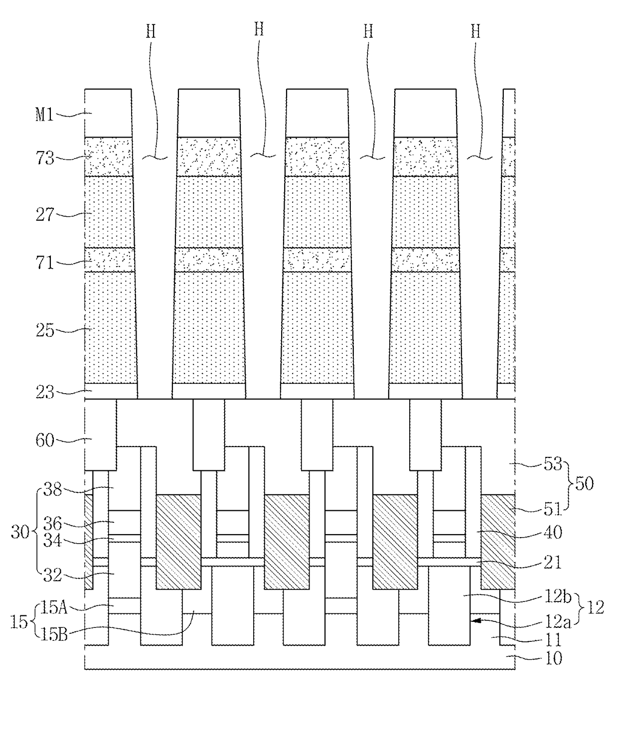
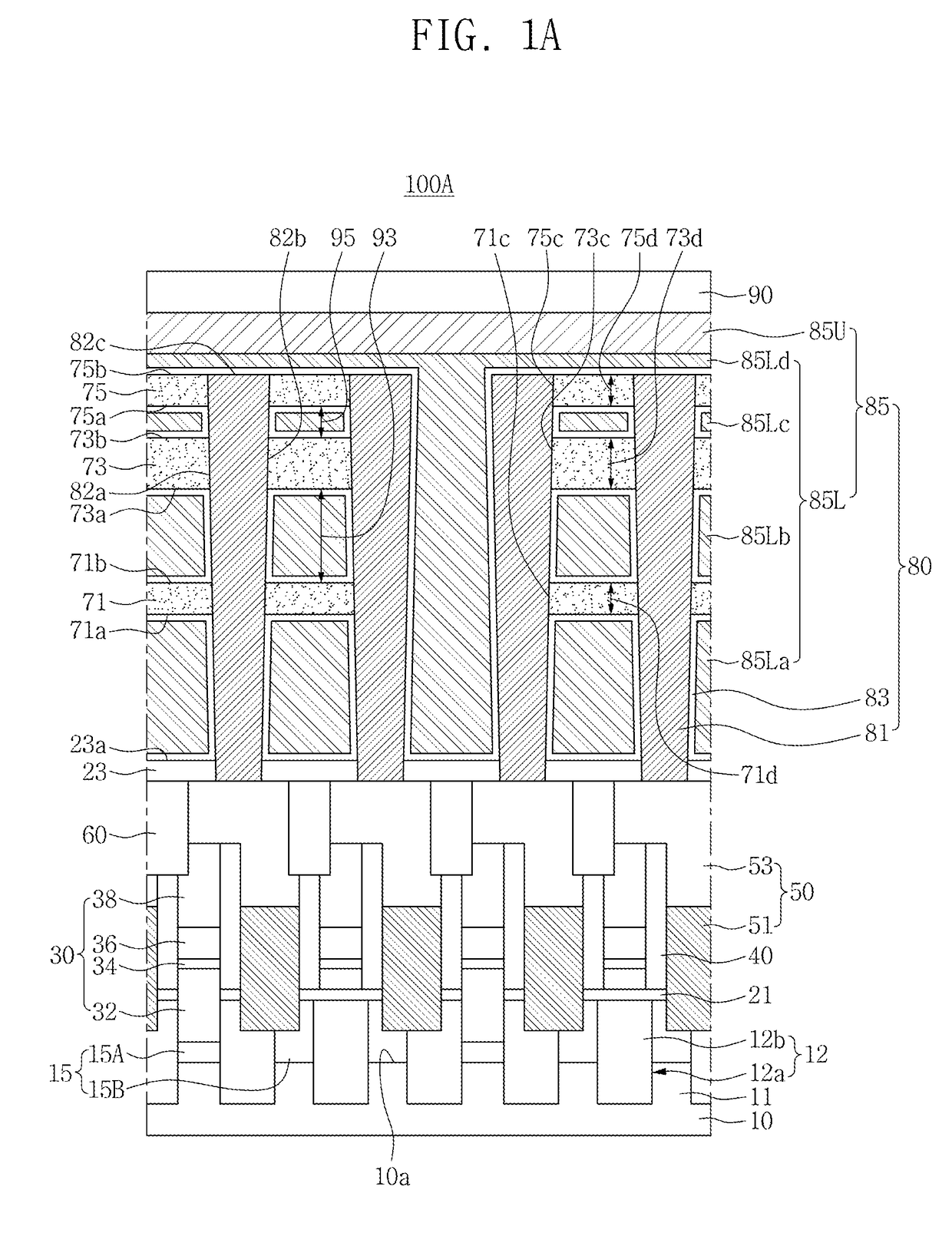
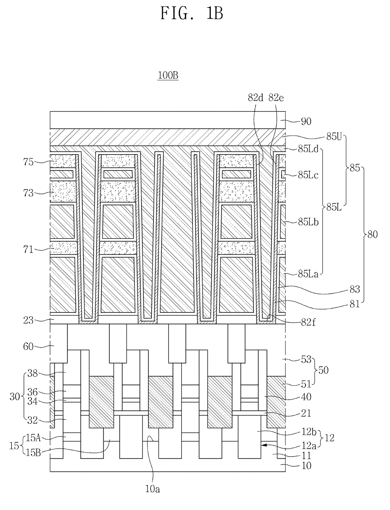
[0040]One or more example embodiments will be described in detail with reference to the accompanying drawings. Example embodiments, however, may be embodied in various different forms, and should not be construed as being limited to only the illustrated embodiments. Rather, the illustrated embodiments are provided as examples so that this disclosure will be thorough and complete, and will fully convey the concepts of this disclosure to those skilled in the art. Accordingly, known processes, elements, and techniques, may not be described with respect to some example embodiments. Unless otherwise noted, like reference characters denote like elements throughout the attached drawings and written description, and thus descriptions will not be repeated.

[0041]Although the terms “first,”“second,”“third,” etc., may be used herein to describe various elements, components, regions, layers, and / or sections, these elements, components, regions, layers, and / or sections, should not be limited by t...


PUM


Abstract

A semiconductor device includes storage electrodes on a substrate and one or more supporters configured to couple one or more portions of the storage electrodes. The semiconductor device may include multiple non-intersecting supporters extending in parallel to a surface of the substrate. At least one supporter may have an upper surface that is substantially coplanar with upper surfaces of the storage electrodes. The storage electrodes may include a capacitor dielectric layer that conformally covers one or more surfaces of the storage electrodes and one or more supporters. A storage electrode may include upper and lower storage electrodes coupled together. The upper and lower storage electrodes may have different horizontal widths.

Description

CROSS-REFERENCE TO RELATED APPLICATION[0001]This application claims priority under 35 U.S.C. §119 to Korean Patent Application No. 10-2015-0129053 filed on Sep. 11, 2015, the disclosure of which is hereby incorporated by reference in its entirety.BACKGROUND[0002]Technical Field[0003]The inventive concepts relate to a semiconductor device having supporters and a method of manufacturing the same.[0004]Description of Related Art[0005]As semiconductor devices have become highly integrated, a design rule thereof have become smaller continuously. Accordingly, an area occupied by a unit cell including one transistor and one capacitor has become smaller gradually. Thus, in some cases it may be difficult to secure a capacitance due to the decrease of the area occupied by the unit cell.SUMMARY[0006]Some example embodiments of the inventive concepts provide semiconductor devices that are configured to provide improved capacitance.[0007]Some example embodiments of the inventive concepts provide...

Claims


Application Information

Patent Timeline
IPC IPC(8): H01L27/108H01L29/06H01L29/45H01L23/522
CPCH01L27/10805H01L29/45H01L29/0649H01L23/5226H10B12/34H10B12/315H10B12/0335H10B12/053
Inventor KIM, KYUNG-EUNKIM, YONGKWANJANG, SEMYEONGCHOI, JAEHYOUNGHWANG, YOOSANGKIM, BONG-SOO
Owner SAMSUNG ELECTRONICS CO LTD
Why Eureka
Try Eureka