Device with Channel Having Varying Carrier Concentration

a field-effect transistor and channel technology, applied in the field of field-effect transistors, can solve the problems of significant limit of performance characteristics, degrade performance, and structure cannot achieve uniform electric field in the device channel, and achieve the effect of increasing the uniformity of electric file distribution

Active Publication Date: 2017-03-16
SENSOR ELECTRONICS TECH
View PDF1 Cites 1 Cited by
  • Summary
  • Abstract
  • Description
  • Claims
  • Application Information

AI Technical Summary

Benefits of technology

[0010]A third aspect of the invention provides a method of fabricating a semiconductor device, the method comprising: creating a semiconductor heterostructure design including: a channel layer; a barrier layer located immediately adjacent to the channel layer; and a device channel formed at an interface of the channel layer and the barrier layer, wherein the creating includes altering at least one attribute of the semiconductor heterostructure design such that the device channel has a carrier concentration that varies laterally along a direction from a location for a gate contact to a location for a drain contact to increase uniformity of an electric filed distribution in a gate-drain region of the semiconductor device; fabricating the semiconductor heterostructure according to the semiconductor heterostructure design; fabricating a gate contact on the semiconductor heterostructure at the location for the gate contact; and fabricating a drain contact on the semiconductor heterostructure at the location for the drain contact.

Problems solved by technology

Although these features make such devices extremely promising for various applications in power electronics, certain material and device specifics significantly limit their performance characteristics.
However, even multiple field plate structures cannot achieve a uniform electric field in the device channel.
Additionally, these approaches can degrade performance due to excessive capacitances associated with the field-plate electrodes.

Method used


Image

  • Device with Channel Having Varying Carrier Concentration
  • Device with Channel Having Varying Carrier Concentration
  • Device with Channel Having Varying Carrier Concentration

Examples


Embodiment Construction

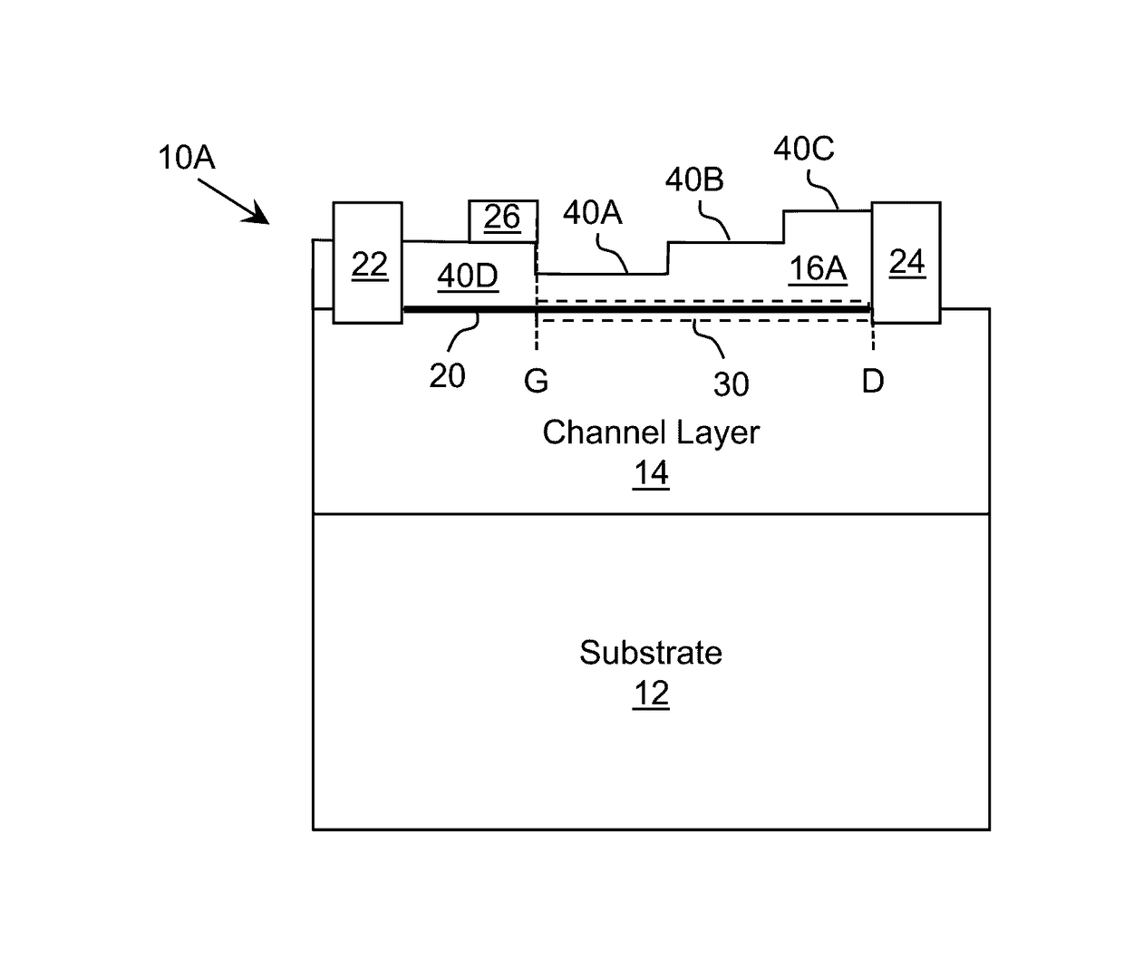
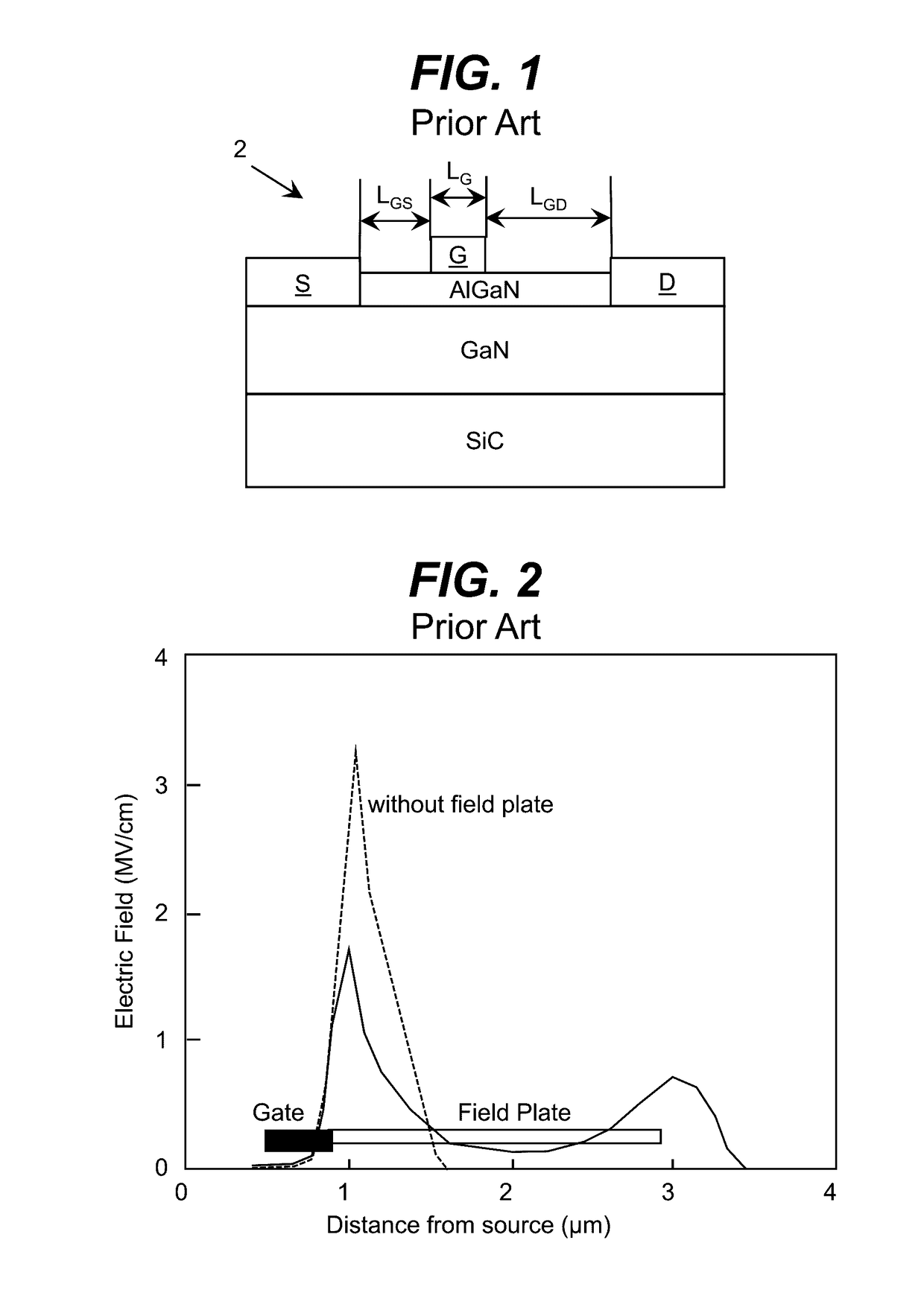
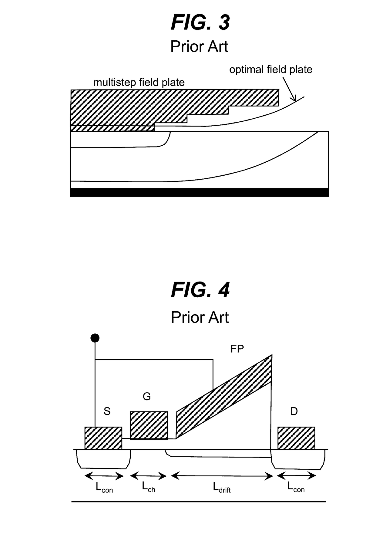
[0025]As indicated above, aspects of the invention provide a semiconductor device including a device channel with a gate-drain region having a carrier concentration that varies laterally along a direction from the gate contact to the drain contact. Lateral variation of the carrier concentration can be implemented by laterally varying one or more attributes of one or more layers located in the gate-drain region of the device. The lateral variation can be configured to increase uniformity of an electric filed distribution in a gate-drain region of the semiconductor device. The increased uniformity can result in a higher breakdown voltage for the device as compared to comparable devices with uniform carrier concentration in the device channel.

[0026]As used herein, unless otherwise noted, the term “set” means one or more (i.e., at least one) and the phrase “any solution” means any now known or later developed solution. It is understood that, unless otherwise specified, each value is app...


PUM


Abstract

A semiconductor device including a device channel with a gate-drain region having a carrier concentration that varies laterally along a direction from the gate contact to the drain contact is provided. Lateral variation of the carrier concentration can be implemented by laterally varying one or more attributes of one or more layers located in the gate-drain region of the device.

Description

REFERENCE TO RELATED APPLICATIONS[0001]The current application claims the benefit of U.S. Provisional Application No. 62 / 218,035, which was filed on 14 Sep. 2015, and which is hereby incorporated by reference.TECHNICAL FIELD[0002]The disclosure relates generally to field-effect transistors, and more particularly, to a field-effect transistor with a significantly improved breakdown voltage.[0003]BACKGROUND ART[0004]High power field-effect transistors (FETs), such as gallium nitride (GaN) based heterostructure field effect transistors (HFETs), feature increasingly high powers and breakdown voltages. Although these features make such devices extremely promising for various applications in power electronics, certain material and device specifics significantly limit their performance characteristics.[0005]On important limitation of GaN-based HFETs, as well as other FETs operating at high voltage, is a non-uniform electric field profile present in the gate-drain spacing. FIG. 1 shows a co...

Claims


Application Information

Patent Timeline
Patent Type & Authority Applications(United States)
IPC IPC(8): H01L29/778H01L29/66H01L29/20
CPCH01L29/7786H01L29/66431H01L29/2003H01L29/0657H01L29/1037H01L29/1045H01L29/201H01L29/41758H01L29/42316
Inventor SIMIN, GRIGORYSHUR, MICHAELDOBRINSKY, ALEXANDER
Owner SENSOR ELECTRONICS TECH
Why Eureka
Try Eureka