
Manufacture method of metal-silicon oxide-metal capacitor

A technology of metal capacitors and manufacturing methods, applied in the field of microelectronics, can solve the problems of MIM capacitor breakdown voltage, leakage current difference, and poor uniformity of silicon nitride film, so as to improve electrical uniformity, reduce silicon-hydrogen bonds, and increase capacitance Effect

Inactive Publication Date: 2012-10-03
SHANGHAI HUALI MICROELECTRONICS CORP
View PDF4 Cites 0 Cited by
  • Summary
  • Abstract
  • Description
  • Claims
  • Application Information

AI Technical Summary

Problems solved by technology

For example, using the PEVCD method, the silicon oxide film is formed by the reaction of silane and nitrous oxide. However, a large number of silicon-hydrogen bonds (Si-H) remain in the silicon oxide film produced by the PECVD method, so that there are more charges in it. This leads to poor uniformity of the silicon nitride film in terms of electrical thickness, and correspondingly poor electrical characteristics such as breakdown voltage and leakage current of the MIM capacitor made of the silicon oxide film.

Method used


Image

  • Manufacture method of metal-silicon oxide-metal capacitor
  • Manufacture method of metal-silicon oxide-metal capacitor
  • Manufacture method of metal-silicon oxide-metal capacitor

Examples


Embodiment Construction

[0025] The present invention will be further described below in combination with principle diagrams and specific operation examples.

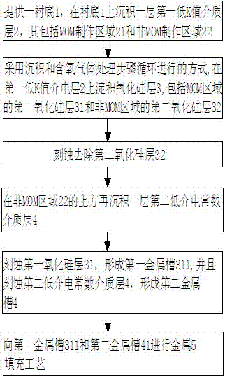
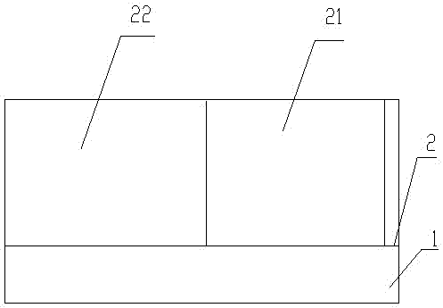
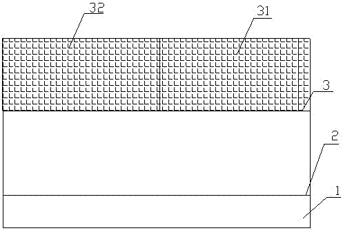
[0026] Such as figure 1 as well as Figures 2A-2H Shown in, the manufacture method of a kind of metal-silicon oxide-metal capacitor of the present invention specifically comprises the following steps:

[0027] Step S1: Provide a substrate 1, and deposit a layer of first low dielectric constant (low K value) dielectric layer 2 on the substrate 1, the surface of the first low dielectric constant dielectric layer 2 includes metal-oxide- metal (MOM) region 21 and non-metal-oxide-metal (non-MOM) region 22;

[0028] Step S2: Deposit a layer of silicon oxide layer 3 on the surface of the first low dielectric constant layer 2, the silicon oxide layer 3 is included in the first silicon oxide layer 31, which is located in the metal-oxide-metal (MOM) region 21 and A second silicon oxide layer 32 in the non-metal-oxide-metal (non-MOM) region. In this s...


PUM


Abstract

The invention discloses a manufacture method of a metal-silicon oxide-metal capacitor. The manufacture method comprises the following steps of: providing a substrate; depositing a first low-dielectric-constant dielectric layer on the substrate, wherein the first low-dielectric-constant dielectric layer comprises a metal-oxide-metal manufacture area and a nonmetal-oxide-metal manufacture area; depositing a silicon oxide layer on the first low-dielectric-constant dielectric layer via the way of circularly depositing and processing oxygen-containing gas, wherein the silicon oxide layer comprises the first silicon oxide layer of the metal-oxide-metal manufacture area and the second silicon oxide layer of the nonmetal-oxide-metal manufacture area; etching the second silicon oxide layer; depositing a second low-dielectric-constant dielectric layer on the nonmetal-oxide-metal manufacture area; etching the first silicon oxide layer to form a first metallic channel, and etching the second low-dielectric-constant dielectric layer to form a second metallic channel; and performing a metal filling process to the first metallic channel and the second metallic channel. The invention improves the electrical characteristics and the electrical uniformity of the capacitor.

Description

technical field [0001] The invention relates to the field of microelectronics, in particular to a method for manufacturing a metal-silicon oxide-metal capacitor. Background technique [0002] Capacitors are important components in integrated circuits and are widely used in memory, microwave, radio frequency, smart card, high voltage and filter chips. A widely used capacitor configuration in chips is metal-insulator-metal (MIM) parallel to the silicon substrate. Among them, the metal is copper, aluminum, etc., whose manufacturing process is easily compatible with the metal interconnection process, and the insulator is a dielectric material with a high dielectric constant (k) such as silicon nitride and silicon oxide. Improving the properties of high-k dielectric materials is one of the main methods to improve capacitor performance. [0003] Plasma Enhanced Chemical Vapor Deposition (PECVD, Plasma Enhanced Chemical Vapor Deposition) is widely used for thin film deposition in...

Claims


Application Information

Patent Timeline
Patent Type & Authority Applications(China)
IPC IPC(8): H01L21/02
Inventor 毛智彪胡友存徐强
Owner SHANGHAI HUALI MICROELECTRONICS CORP
Learn More