Semiconductor optical waveguide, semiconductor optical mudulator, and semiconductor optical modulation system

a technology of semiconductor optical mudulator and semiconductor optical waveguide, which is applied in the field of semiconductor optical mudulator and semiconductor optical modulation system, can solve the problems of difficult to avoid deterioration of high frequency characteristics, difficult to secure and achieve the effect of improving modulation efficiency and ensuring both modulation efficiency and high frequency characteristics

Inactive Publication Date: 2017-04-13
THE FUJIKURA CABLE WORKS LTD
View PDF7 Cites 4 Cited by
  • Summary
  • Abstract
  • Description
  • Claims
  • Application Information

AI Technical Summary

Benefits of technology

The present invention enables a semiconductor optical waveguide to have both high efficiency and good performance at high frequencies. This also allows for further improvement in modulation efficiency.

Problems solved by technology

However, the semiconductor optical waveguide described in Patent Literature 1 has a problem that it is difficult to avoid deterioration of high frequency characteristics.
It is thus difficult to secure both modulation efficiency and high frequency characteristics in the semiconductor optical waveguide described in Patent Literature 1.

Method used


Image

  • Semiconductor optical waveguide, semiconductor optical mudulator, and semiconductor optical modulation system
  • Semiconductor optical waveguide, semiconductor optical mudulator, and semiconductor optical modulation system
  • Semiconductor optical waveguide, semiconductor optical mudulator, and semiconductor optical modulation system

Examples


embodiment 1

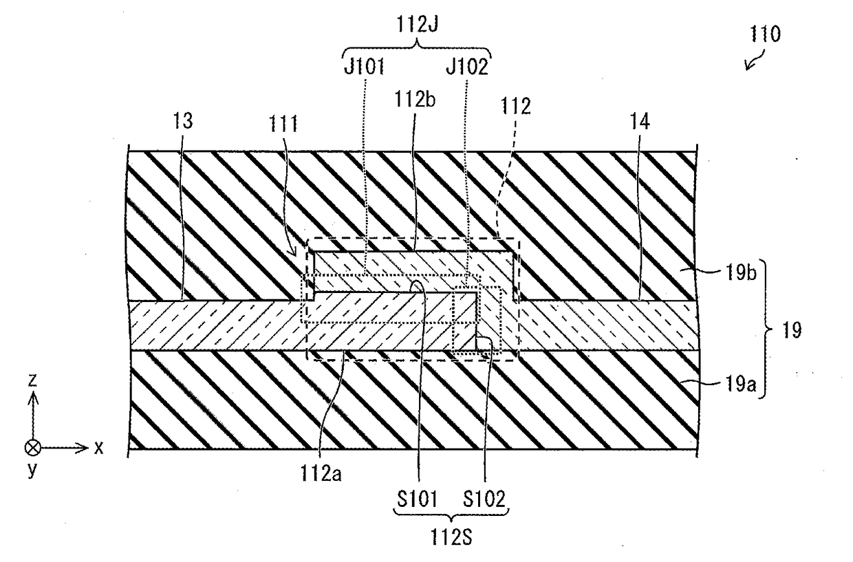
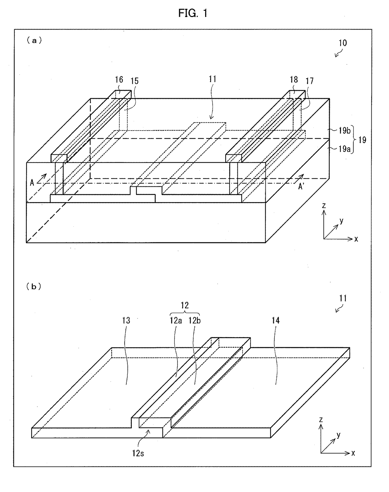
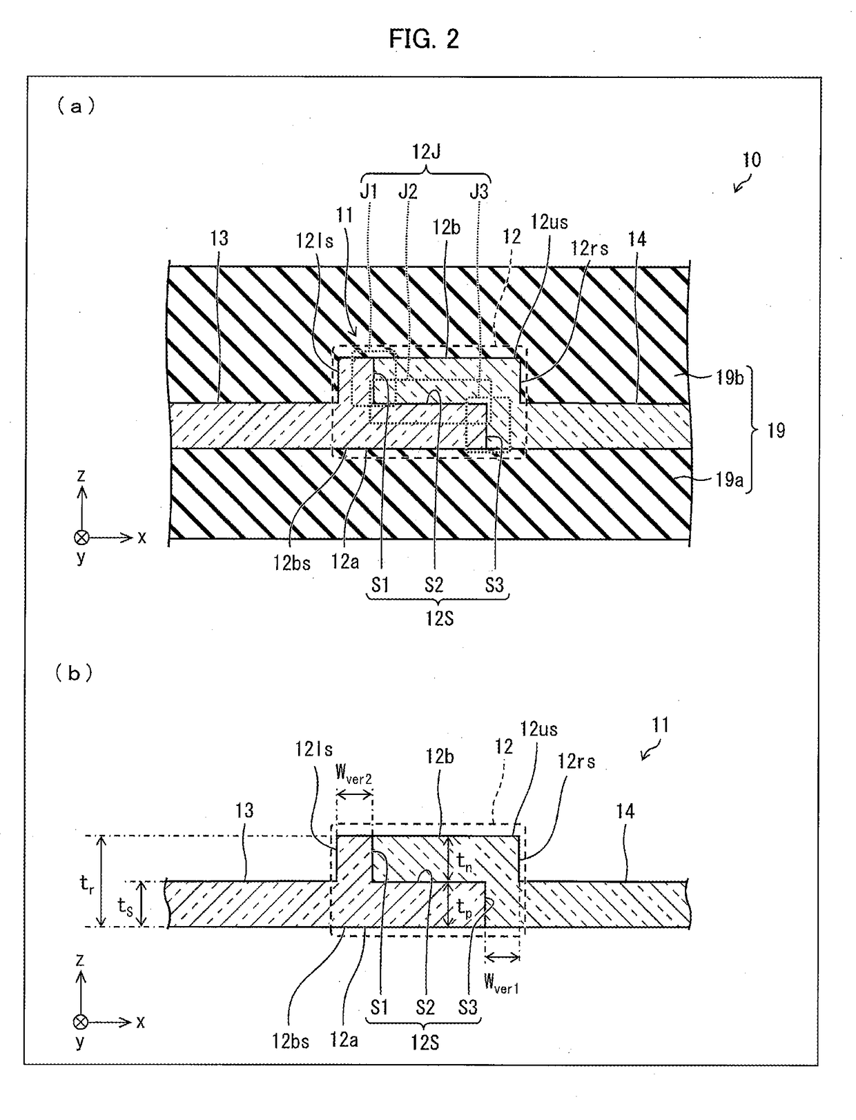
[0042]A semiconductor optical waveguide 10 in accordance with Embodiment 1 of the present invention is described with reference to FIGS. 1 and 2. (a) of FIG. 1 is a perspective view illustrating a configuration of the semiconductor optical waveguide 10. (b) of FIG. 1 is a perspective view illustrating a configuration of a core 11 included in the semiconductor optical waveguide 10. (a) of FIG. 2 is a partial cross-sectional view of a part of a cross section taken along a line A-A′ in (a) of FIG. 1 and illustrating a configuration of the semiconductor optical waveguide 10. (b) of FIG. 2 is a partial cross-sectional view of a part of the cross section taken along the line A-A′ in (a) of FIG. 1 and illustrating a configuration of the core 11 included in the semiconductor optical waveguide 10. The cross section taken along the line A-A′ in (a) of FIG. 1 is a cross section (x-z plane) that is perpendicular to a direction (y direction) in which light is guided in a rib 12.

[0043](Configurat...

modified example 1

[0087]The following description will discuss, with reference to (a) of FIG. 3, Modified Example 1 of the semiconductor optical waveguide 10 in accordance with Embodiment 1. (a) of FIG. 3 is a cross-sectional view illustrating a configuration of a core 11 included in a semiconductor optical waveguide 10 in accordance with Modified Example 1.

[0088]The semiconductor optical waveguide 10 in accordance with Modified Example 1 is obtained by configuring the semiconductor optical waveguide 10 (see (b) of FIG. 2) in accordance with Embodiment 1 such that the thickness tp of the p-type semiconductor region 12a is greater than the thickness tn of the n-type semiconductor region 12b.

[0089]Note that in the Description, a center of the rib 12 is defined as a position at which a plane obtained by equally dividing the rib 12 along a height (a width between the lower surface 12bs and the upper surface 12us) of the rib 12 and another plane obtained by equally dividing the rib 12 along a width (a wi...

modified example 2

[0097]Modified Example 2 of the semiconductor optical waveguide 10 in accordance with Embodiment 1 is described with reference to (b) of FIG. 3. (b) of FIG. 3 is a cross-sectional view illustrating a core 11 included in a semiconductor optical waveguide 10 in accordance with Modified Example 2.

[0098]The semiconductor optical waveguide 10 in accordance with Modified Example 2 is obtained by configuring the semiconductor optical waveguide 10 in accordance with Embodiment 1 (see (b) of FIG. 2) such that (1) the thickness tp is greater than the thickness tn and (2) the width Wver2 is smaller than the thickness tn. In other words, the semiconductor optical waveguide 10 in accordance with Modified Example 2 is obtained by configuring the semiconductor optical waveguide 10 in accordance with Modified Example 1 such that the width Wver2 is smaller than the thickness tn.

[0099]According to this configuration, in a case where a p-n junction 12J having a junction surface 12S with a crank shape ...


PUM


Abstract

A boundary surface (12S) which divides a rib (12) of a rib-slab type core (11) into a p-type semiconductor region (12a) and an n-type semiconductor region (12b) is constituted by a first flat surface (S1) serving as a junction surface of a first lateral p-n junction (J1), a second flat surface (S2) serving as a junction surface of a vertical p-n junction (J2), and a third flat surface (S3) serving as a junction surface of a second lateral p-n junction (J3).

Description

[0001]This Nonprovisional application claims priority under 35 U.S.C. §119 on Patent Application No. 2015-201477 filed in Japan on Oct. 9, 2015, the entire contents of which are hereby incorporated by reference.TECHNICAL FIELD[0002]The present invention relates to a semiconductor optical waveguide which includes a core having a p-type semiconductor region and an n-type semiconductor region. The present invention also relates to a semiconductor optical modulator including the semiconductor optical waveguide, and a semiconductor optical modulation system including the semiconductor optical modulator.BACKGROUND ART[0003]There is known a semiconductor optical waveguide having a core made of a semiconductor (e.g., silicon). It is also known that a semiconductor optical waveguide which includes a core having a p-type semiconductor region and an n-type semiconductor region functions as a phase modulator which modulates a phase of light near a junction surface of a p-n junction. A phase of ...

Claims


Application Information

Patent Timeline
IPC IPC(8): G02F1/025G02F1/225G02F1/01H01L29/167
CPCG02F1/025H01L29/167G02F1/2257G02F2001/212G02F1/0123G02F2201/127G02F1/2255G02F2201/063G02F1/212
Inventor SAKAMOTO, SHINICHIISHIKURA, NORIHIRO
Owner THE FUJIKURA CABLE WORKS LTD
Why Eureka
Try Eureka