Semiconductor device simulation

a technology of mikro-conductor and simulation, applied in the field of mikro-conductor devices, can solve the problems of high cost and time consumption, the use of traditional cmos drift-diffusion tcad in advanced cmos has become questionable, and the development of comprehensive mobility models has become a very expensive and time-consuming task

Active Publication Date: 2017-04-13
SYNOPSYS INC
View PDF2 Cites 6 Cited by
  • Summary
  • Abstract
  • Description
  • Claims
  • Application Information

AI Technical Summary

Problems solved by technology

However the usefulness of the traditional drift-diffusion TCAD in advanced CMOS has become questionable.
The development of comprehensive mobility models, which are at the heart of any drift-diffusion TCAD simulators, has become a very expensive and time consuming task.
Having all necessary measurements to inform the mobility model development and parameter extraction becomes difficult, computationally expensive and slow.
Having them before the corresponding FinFET technology is developed is practically impossible.
The problem is exacerbated for transistors with new channel materials such as SiGe, Ge or III-Vs, rendering the use of drift-diffusion for screening of new technology options practically impossible.
If 50 years of silicon CMOS were not enough to develop all-encompassing silicon mobility models, the prospects for developing predictive simulations for transistors with new channel materials using conventional approaches are poor.
Furthermore, even if accurate low-field mobility models in the above cases were to be developed using conventional approaches, their value for predictive drift-diffusion simulation of transistor performance at high drain bias conditions is very limited.
However EMC simulations are slow, noisy and expensive.
However, it is not practical to perform the required comprehensive EMC simulations for any new transistor geometry, new substrate or channel orientation, new strain conditions, new channel materials, etc.

Method used


Image

  • Semiconductor device simulation
  • Semiconductor device simulation
  • Semiconductor device simulation

Examples


Embodiment Construction

[0046]The present invention is directed to a method and system of simulating semiconductor devices. The following description contains specific information pertaining to the implementation of the present invention. One skilled in the art will recognize that the present invention may be implemented in a manner different from that specifically discussed in the present application. Moreover, some of the specific details of the invention are not discussed in order not to obscure the invention.

[0047]The drawings in the present application and their accompanying detailed description are directed to merely exemplary embodiments of the invention. To maintain brevity, other embodiments of the present invention are not specifically described in the present application and are not specifically illustrated by the present drawings.

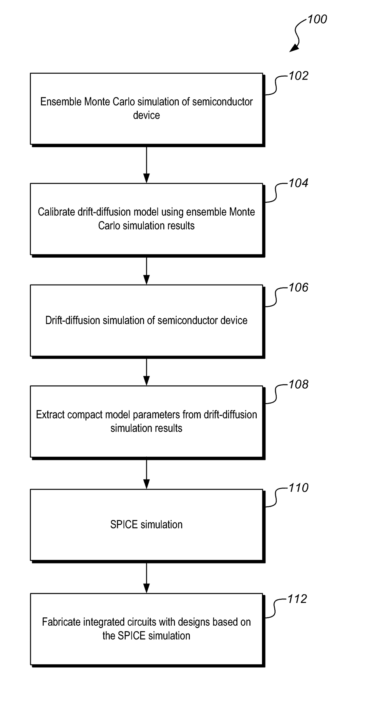
[0048]With reference to FIG. 1, a flowchart 100 illustrates typical steps taken to implement a conventional method in which EMC and drift-diffusion simulations are use...


PUM


Abstract

In one embodiment, a method for simulating semiconductor devices includes the steps: running ensemble Monte Carlo (EMC) simulations of a plurality of semiconductor devices having a first plurality of configurations in a Design of Experiment (DoE) space to produce EMC results; extracting mobility parameters across the DoE space from the EMC results; constructing a response-surface mobility model using the extracted mobility parameters; and using the response-surface mobility model to run a drift-diffusion simulation of a semiconductor device with a different configuration from the first plurality of configurations.

Description

CROSS REFERENCE TO RELATED APPLICATIONS[0001]The present invention claims priority to U.S. Provisional Application No. 62 / 239,235, entitled “Semiconductor Device Simulation” and filed on Oct. 8, 2015, the entirety of which is being incorporated by reference herein. The present application may also be related to U.S. patent application Ser. No. ______, entitled “Parameter Generation for Semiconductor Device Trapped-Charge Modeling” and filed on May 9, 2016, which, in turn, claims priority to U.S. Provisional Application No. 62 / 163,924, entitled “Parameter Generation for Semiconductor Device Trapped-Charge Modeling” and filed on May 19, 2015, the entirety of both of which is being incorporated by reference herein. The present application may also be related to U.S. patent application Ser. No. ______, entitled “Parameter Generation for Modeling of Process-Induced Semiconductor Device Variation” and filed on May 9, 2016, which, in turn, claims priority to U.S. Provisional Application No...

Claims


Application Information

Patent Timeline
Patent Type & Authority Applications(United States)
IPC IPC(8): G06F17/50G06F17/18
CPCG06F17/18G06F17/5036G06F30/367G06F2111/08G06F30/20G06F30/23G06F2111/10
Inventor ASENOV, ASEN
Owner SYNOPSYS INC
Why Eureka
Try Eureka