Electronic component

Active Publication Date: 2017-04-20
MURATA MFG CO LTD
View PDF8 Cites 23 Cited by
  • Summary
  • Abstract
  • Description
  • Claims
  • Application Information

AI Technical Summary

Benefits of technology

[0010]According to a preferred embodiment of the present invention, an electronic component is able to be mounted on a ci

Problems solved by technology

However, it is difficult to mount the electronic component 500 disclosed in Japanese Unexamined Patent A

Method used


Image

  • Electronic component
  • Electronic component
  • Electronic component

Examples


first preferred embodiment

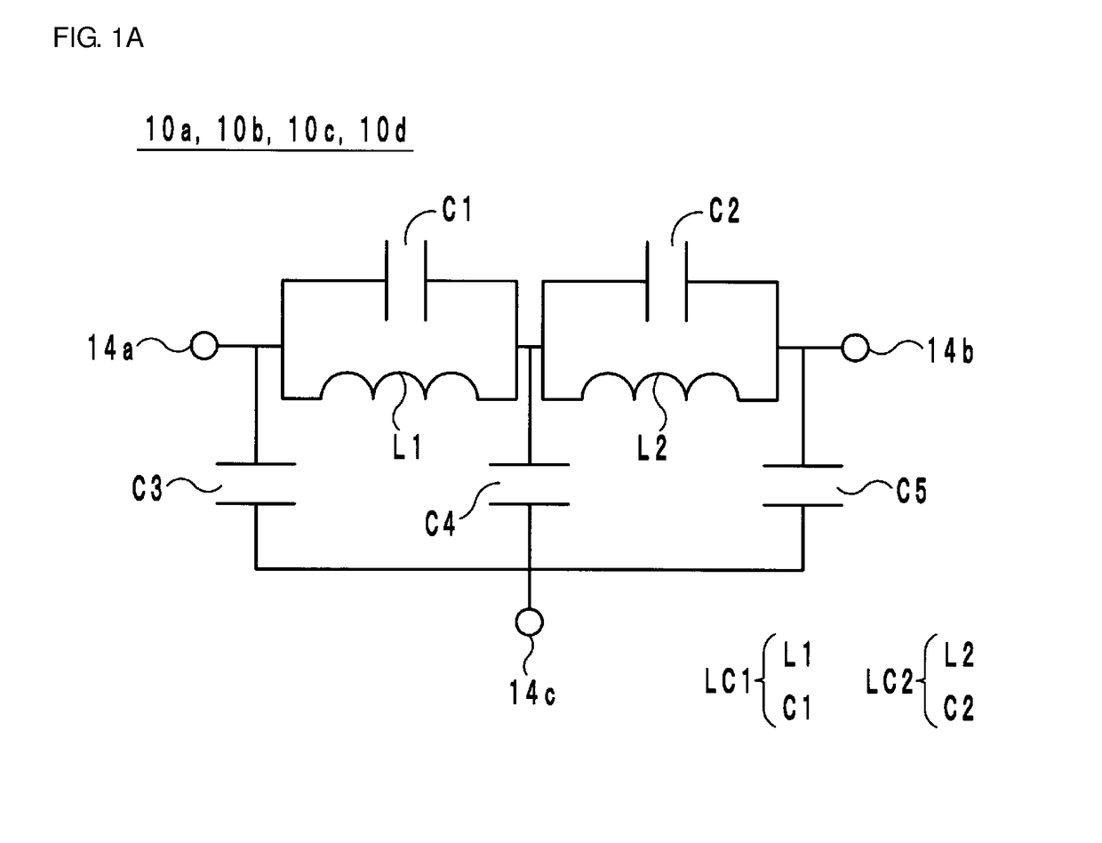
[0021]Hereafter, an electronic component according to a first preferred embodiment of the present invention will be described while referring to the drawings. FIG. 1A is an equivalent circuit diagram of electronic components 10a to 10d according to the preferred embodiments of the present invention.

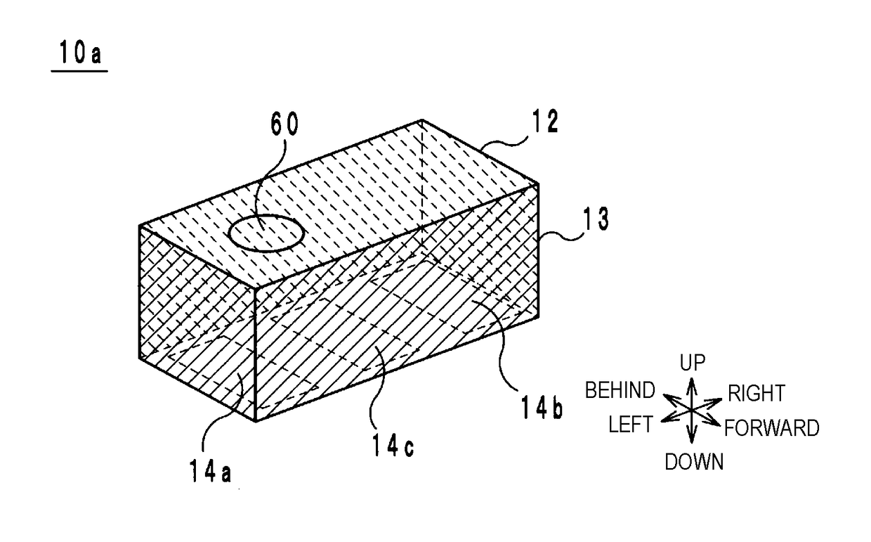
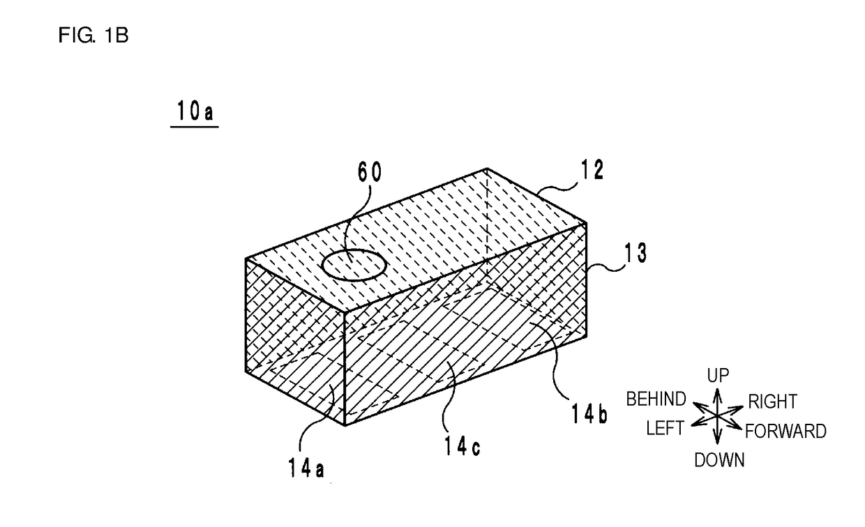
[0022]The electronic component 10a preferably includes a low pass filter that includes a plurality of passive elements. As illustrated in FIG. 1A, the electronic component 10a includes LC parallel resonators LC1 and LC2, capacitors C3 to C5 (examples of passive elements) and outer electrodes 14a to 14c. The outer electrodes 14a and 14b are input / output outer electrodes through which high-frequency signals are input and output and the outer electrode 14c is a ground outer electrode that is connected to the ground potential.

[0023]The LC parallel resonators LC1 and LC2 are serially connected to each other in this order between the outer electrode 14a and the outer electrode 14b. The LC paral...

second preferred embodiment

[0064]Hereafter, an electronic component according to a second preferred embodiment of the present invention will be described while referring to the drawings. FIG. 4 is an external perspective view of an electronic component 10b according to the second preferred embodiment of the present invention. An equivalent circuit diagram and an exploded perspective view of the electronic component 10b are the same or substantially the same as those of the electronic component 10a and therefore FIG. 1A and FIG. 2 will be referred to here.

[0065]The shape of the shield electrode 13 of the electronic component 10b is different from the shape of the shield electrode 13 of the electronic component 10a. Hereafter, the electronic component 10b will be described while focusing on this difference.

[0066]As illustrated in FIG. 4, in the electronic component 10b, the shield electrode 13 preferably does not extend up to the top surface and the bottom surface of the multilayer body 12. That is, there is a ...

third preferred embodiment

[0071]Hereafter, an electronic component according to a third preferred embodiment of the present invention will be described while referring to the drawings. FIG. 5 is an external perspective view of an electronic component 10c according to the third preferred embodiment of the present invention. An equivalent circuit diagram of the electronic component 10c is the same or substantially the same as the equivalent circuit diagram of the electronic component 10a and therefore FIG. 1A will be referred to.

[0072]The electronic component 10c differs from the electronic component 10a in terms of the shape of the shield electrode 13 and presence / absence of the ground conductor layers 50 and 52a to 52d. Hereafter, the electronic component 10c will be described while focusing on these differences.

[0073]As illustrated in FIG. 5, the shield electrode 13 is preferably also provided on the top surface of the multilayer body 12 in addition to the four side surfaces of the multilayer body 12. In th...


PUM


Abstract

An electronic component includes a main body, an inner conductor inside the main body, one or more outer electrodes on a bottom surface of the main body and not provided on four side surfaces of the main body, and a shield electrode covering the four side surfaces of the main body and having a cylindrical or substantially cylindrical shape, the shield electrode not being physically connected to any of the one or more outer electrodes at a surface of the main body and being connected to the inner conductor at a surface of the main body.

Description

CROSS REFERENCE TO RELATED APPLICATIONS[0001]This application claims the benefit of priority to Japanese Patent Application 2015-204719 filed on Oct. 16, 2015, the entire contents of which application are hereby incorporated herein by reference.BACKGROUND OF THE INVENTION[0002]1. Field of the Invention[0003]The present invention relates to an electronic component in which an outer electrode is included on a bottom surface thereof.[0004]2. Description of the Related Art[0005]For example, a shielded multilayer electronic component (hereafter, simply referred to as “electronic component”) disclosed in Japanese Unexamined Patent Application Publication No. 9-121093 is known as an example of an invention relating to an electronic component of the related art. FIG. 7 is an external perspective view of an electronic component 500 disclosed in Japanese Unexamined Patent Application Publication No. 9-121093.[0006]As illustrated in FIG. 7, the electronic component 500 includes a main body 502...

Claims


Application Information

Patent Timeline
IPC IPC(8): H01F27/34H01F27/28H01G4/40H05K9/00H01G4/30
CPCH01F27/34H05K9/0064H05K9/0081H01F2027/2809H01G4/40H01F27/2804H01G4/30H03H5/02H01F17/0013H01F27/292H01F2017/0026H01F2017/008H01G4/012H01G4/224
Inventor MASUDA, YUTAKAMIYAHARA, KUNIHIROMATSUSHITA, YOSUKE
Owner MURATA MFG CO LTD
Why Eureka
Try Eureka