Capacitive force sensing touch panel

a capacitance force and touch panel technology, applied in the field of touch panel, can solve the problems of inaccurate force sensing results, force sensing determined according to capacitance variation, etc., and achieve the effect of avoiding noise interference of liquid crystal modules and being thinner and lighter

Inactive Publication Date: 2017-04-27
RAYDIUM SEMICON
View PDF9 Cites 16 Cited by
  • Summary
  • Abstract
  • Description
  • Claims
  • Application Information

AI Technical Summary

Benefits of technology

[0037]In an embodiment, a touch sensing mode and a force sensing mode of the capacitive force sensing touch panel are driven in the same amplitude, the same phase or the same frequency to reduce a driving loading of the touch sensing mode and the force sensing mode without reducing touch and force sensing times.
[0040]Compared to the prior art, the capacitive force sensing touch panel of the invention has the following advantages and effects:
[0041](1) Although touch sensing and force sensing both use capacitance variation as judgment basis, the invention uses a relative upper electrode to avoid the effects caused by the change of finger pressing area to maintain the accurate sensed capacitance during the force sensing period.
[0042](2) The capacitive force sensing touch panel of the invention can be applied to in-cell touch panel structure to achieve the effects of thinner and lighter.
[0043](3) Touch sensing and force sensing of the capacitive force sensing touch panel of the invention can be driven in a time-sharing way and operated during the blanking interval of the display period to avoid the noise interference of the liquid crystal module.

Problems solved by technology

Therefore, the force sensing determined according to capacitance variation will be also affected and no accurate force sensing result can be obtained by using the conventional laminated structure of capacitive touch panel shown in FIG. 1.

Method used


Image

  • Capacitive force sensing touch panel
  • Capacitive force sensing touch panel
  • Capacitive force sensing touch panel

Examples


Embodiment Construction

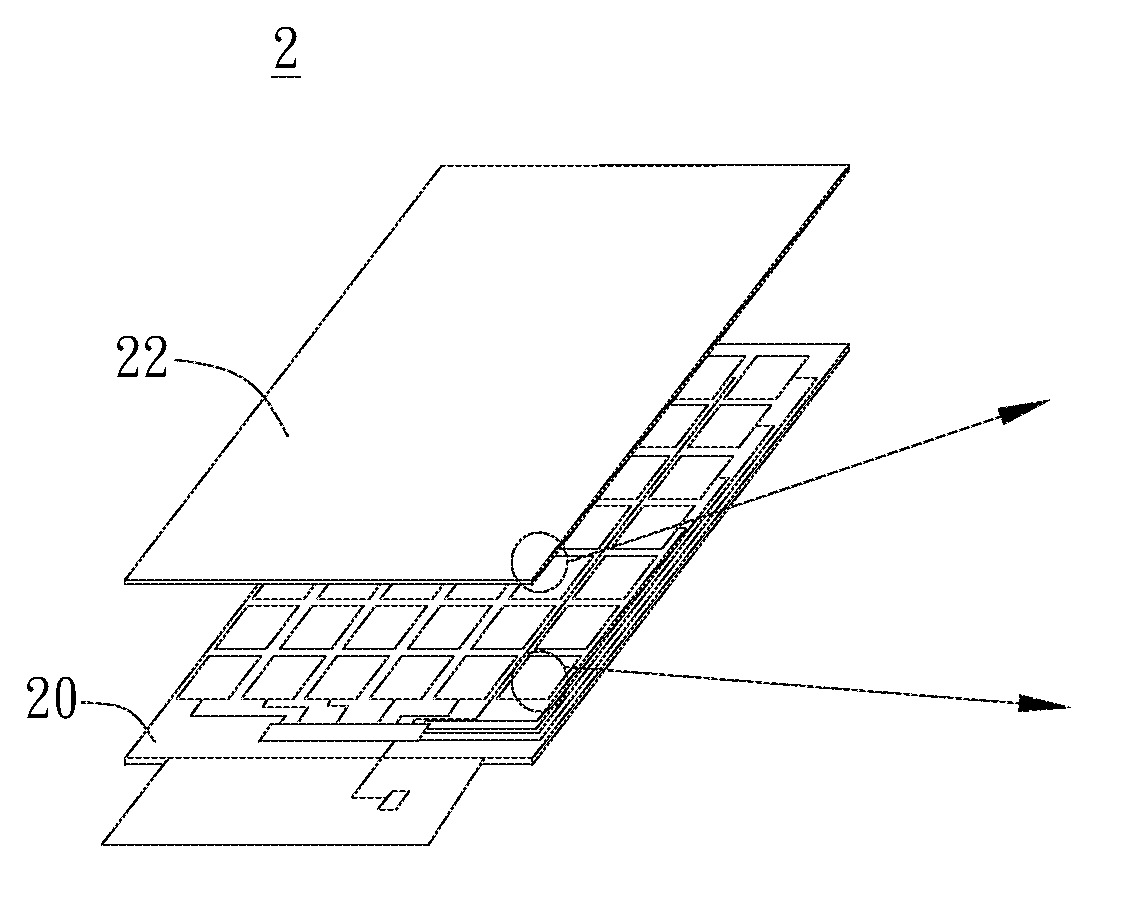
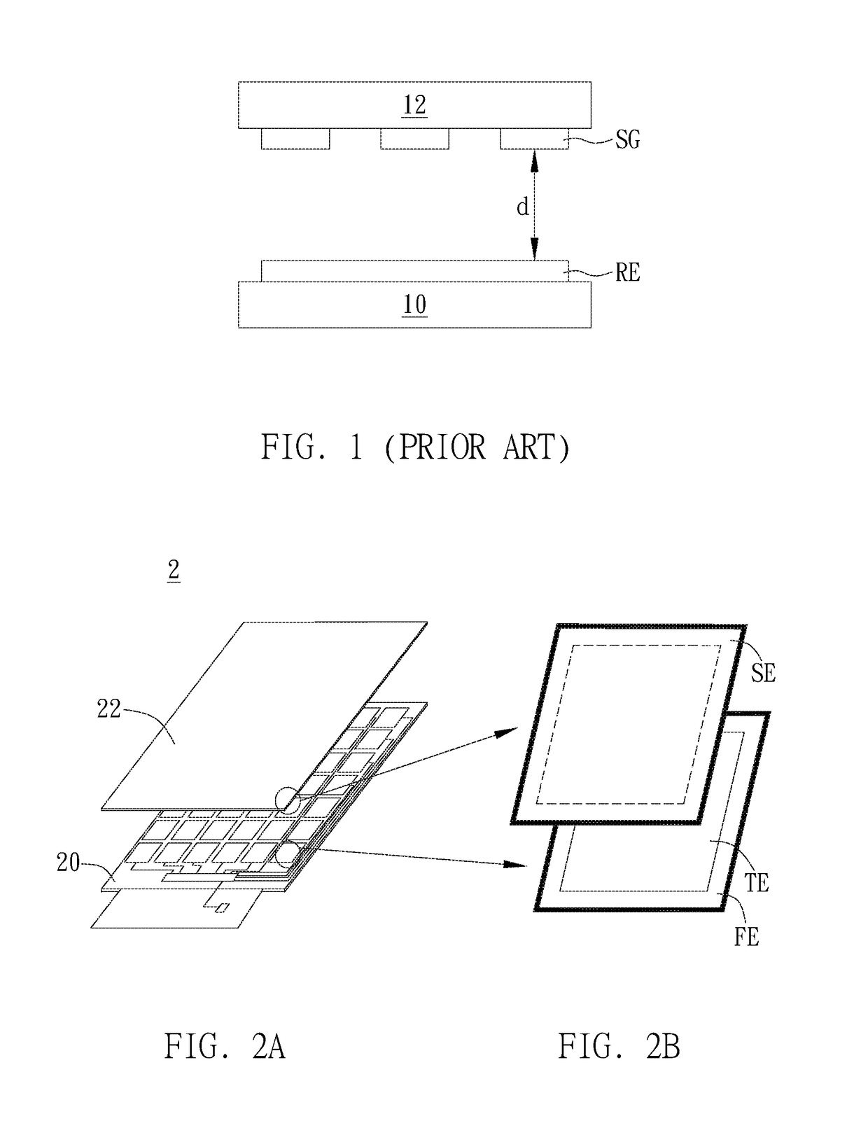
[0063]The invention discloses a capacitive force sensing touch panel which can have an in-cell touch panel structure and use a relative upper shielding electrode to avoid the effects caused by the change of finger pressing area to maintain the accurate sensed capacitance during the force sensing period to improve the drawbacks of the prior arts.

[0064]At first, please refer to FIG. 2A and FIG. 2B. FIG. 2A and FIG. 2B illustrate schematic diagrams of the entire laminated structure and the unit electrode in the laminated structure of the node self-capacitive force sensing touch panel respectively in an embodiment of the invention.

[0065]As shown in FIG. 2A and FIG. 2B, the laminated structure 2 includes a first substrate 20 and a second substrate 22, and the second substrate 22 is disposed above the first substrate 20. In fact, the first substrate 20 and the second substrate 22 can be a TFT glass and a color filter glass respectively, but not limited to this.

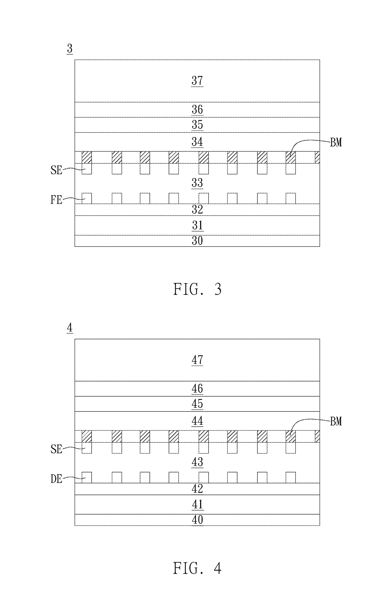
[0066]In this embodiment, a ...


PUM

PropertyMeasurementUnit
conductiveaaaaaaaaaa
capacitive forceaaaaaaaaaa
capacitanceaaaaaaaaaa

Abstract

A capacitive force sensing touch panel is disclosed. The capacitive force sensing touch panel includes pixels. A laminated structure of each pixel includes a first substrate, a TFT layer, a first conductive layer, a second conductive layer, a third conductive layer and a second substrate. The TFT layer is disposed above the first substrate. The first conductive layer is disposed above the TFT layer. The second conductive layer is disposed above the first conductive layer. The third conductive layer corresponds to the second conductive layer and the third conductive layer is disposed above the second conductive layer. The second substrate is disposed above the third conductive layer.

Description

BACKGROUND OF THE INVENTION[0001]1. Field of the Invention[0002]This invention relates to touch panel, especially to a capacitive force sensing touch panel.[0003]2. Description of the Prior Art[0004]In general, if capacitive touch electrodes in a capacitive touch panel are also used to be force sensing electrodes at the same time, such as the sensing electrode SG in FIG. 1 is disposed on the upper substrate 12. And, the reference electrode RE can be disposed on the lower substrate 10 in FIG. 1.[0005]When the upper substrate 12 is pressed by a finger, because the distance d between the sensing electrode SE on the upper substrate 12 and the reference electrode RE on the lower substrate 10 will be changed based on different forces provided by the finger, the capacitance sensed between the sensing electrode SE and the reference electrode RE will be also changed accordingly.[0006]However, the capacitive touch sensing signal will be also changed based on different finger pressing areas. W...

Claims


Application Information

Patent Timeline
Patent Type & Authority Applications(United States)
IPC IPC(8): G06F3/041G02F1/1333G02F1/1368G06F3/044
CPCG06F3/0416G06F3/044G06F3/0412G02F2001/13685G02F1/1368G06F2203/04107G06F2203/04112G02F1/13338G06F3/0414G06F3/0445G06F3/0446G06F3/0447G06F3/04166G02F1/134372
Inventor LIN, YI-YINGSHIEH, HSIN-WEICHIANG, CHANG-CHINGLEE, KUN-PEI
Owner RAYDIUM SEMICON
Why Eureka
Try Eureka