System and method for discharging electrostatic charge in nanoimprint lithography processes

Active Publication Date: 2017-05-04
CANON KK
View PDF4 Cites 7 Cited by
  • Summary
  • Abstract
  • Description
  • Claims
  • Application Information

AI Technical Summary

Benefits of technology

The patent describes an apparatus for imprint lithography processes. It includes an alpha-ionizer and a grounded conductor that work together to create a neutral plasma field and discharge accumulated electric charge from the template and substrate. This rapid discharge helps to meet process parameters for high-throughput imprint lithography. The apparatus also includes an additional alpha-ionizer and conductor for the same purpose. Overall, this technology ensures safe and reliable imprint lithography processes.

Problems solved by technology

The electrostatic charge generated on the template and on the solidified layer, in turn, causes unwanted electrostatic attraction of different kinds of particulates from the air or surrounding environment.
These particulates, once accumulated onto the template or solidified layer, in turn cause defects during subsequent imprinting and / or substrate processing, resulting in reduced imprint quality, device failure, template damage, and other associated problems.
However, such ionized gas is understood to be generated by a corona (or high voltage) discharge from a metal conductor, which itself creates undesirable particles that can migrate to the template surface and cause damage and / or process defects.
There are other techniques for generation of ionized air like x-rays, UV light, γ-radiation that are likewise unsuitable for nanoimprint lithography.
While these techniques do not produce harmful particulates, they still do not produce enough ion concentration in air to yield an effective discharge rate for nanoimprint applications.

Method used


Image

  • System and method for discharging electrostatic charge in nanoimprint lithography processes
  • System and method for discharging electrostatic charge in nanoimprint lithography processes
  • System and method for discharging electrostatic charge in nanoimprint lithography processes

Examples


Embodiment Construction

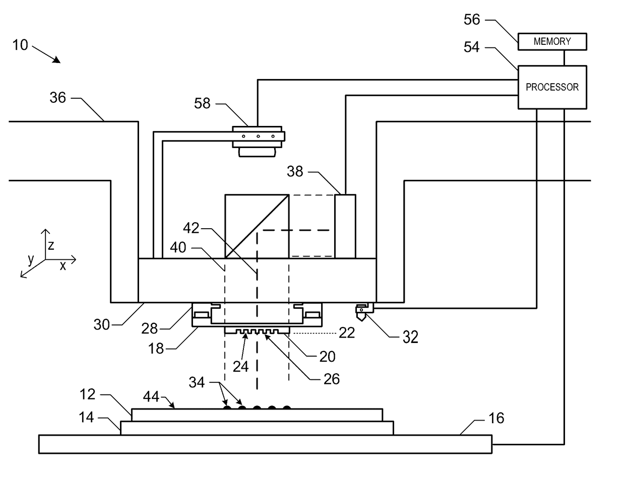
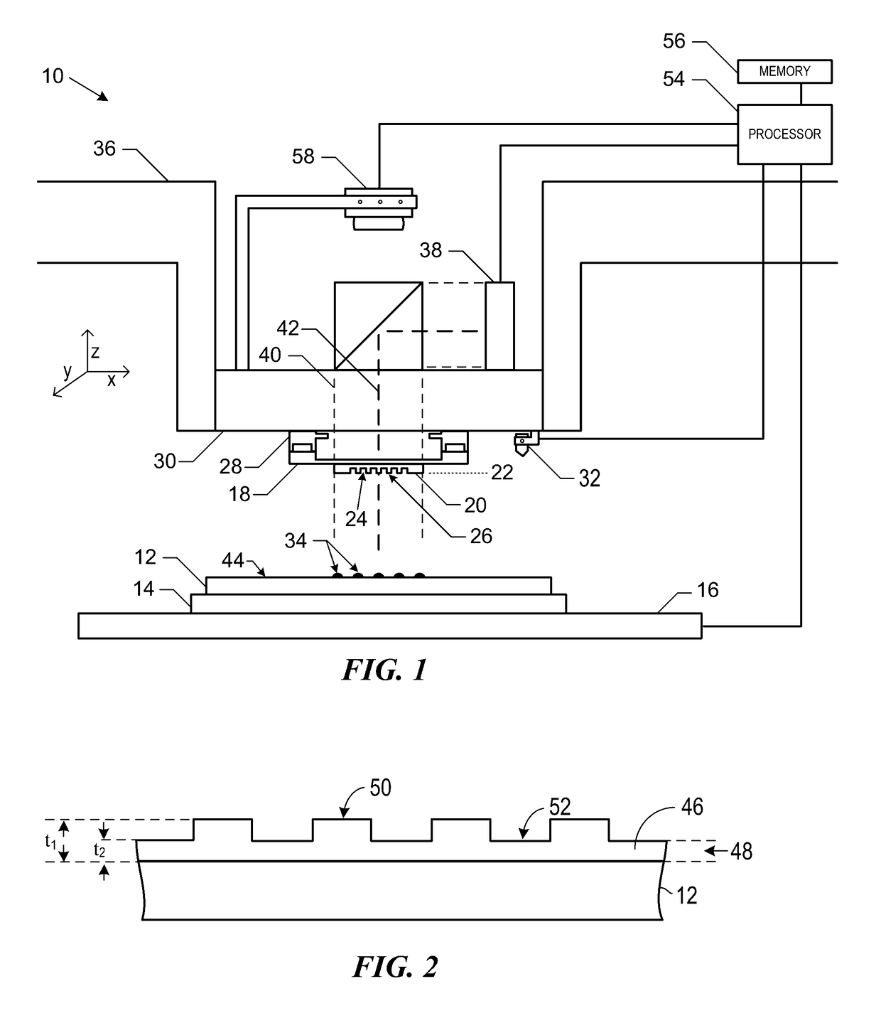
[0020]Referring to the figures, and particularly to FIG. 1, illustrated therein is a nanoimprint lithography system 10 used to form a relief pattern on substrate 12. Substrate 12 may be coupled to substrate chuck 14. As illustrated, substrate chuck 14 is a vacuum chuck. Substrate chuck 14, however, may be any chuck including, but not limited to, vacuum, pin-type, groove-type, electrostatic, electromagnetic, and / or the like. Exemplary chucks are described in U.S. Pat. No. 6,873,087, which is hereby incorporated by reference herein.

[0021]Substrate 12 and substrate chuck 14 may be further supported by stage 16. Stage 16 may provide translational and / or rotational motion along the x, y, and z-axes. Stage 16, substrate 12, and substrate chuck 14 may also be positioned on a base (not shown).

[0022]Spaced-apart from substrate 12 is template 18. Template 18 may include a body having a first side and a second side with one side having a mesa 20 extending therefrom towards substrate 12, with m...


PUM


Abstract

Apparatus, systems and methods that use alpha-ionizers to discharge electrostatic charge accumulated on the working surfaces of imprint lithography templates and / or substrates.

Description

REFERENCE TO RELATED APPLICATION[0001]This patent application claims priority to U.S. Provisional Application Ser. No. 62 / 248,749 filed Oct. 30, 2015, which is incorporated by reference herein in its entirety.BACKGROUND INFORMATION[0002]Nano-fabrication includes the fabrication of very small structures that have features on the order of 100 nanometers or smaller. One application in which nano-fabrication has had a sizeable impact is in the processing of integrated circuits. The semiconductor processing industry continues to strive for larger production yields while increasing the circuits per unit area formed on a substrate; therefore nano-fabrication becomes increasingly important. Nano-fabrication provides greater process control while allowing continued reduction of the minimum feature dimensions of the structures formed. Other areas of development in which nano-fabrication has been employed include biotechnology, optical technology, mechanical systems, and the like.[0003]An exem...

Claims


Application Information

Patent Timeline
IPC IPC(8): B41C1/10
CPCB41C1/1058G03F7/0002
Inventor KHUSNATDINOV, NIYAZ
Owner CANON KK
Why Eureka
Try Eureka