
LED filament

a technology of led filament and filament, which is applied in the direction of elongating light sources, semiconductor devices of light sources, lighting and heating apparatus, etc., can solve the problems of many homeowners not being able to put in compact fluorescent bulbs, and achieve the effects of long service life, extended lifespan, and remarkable energy efficiency

Active Publication Date: 2017-05-11
ZHEJIANG SUPER LIGHTING ELECTRIC APPLIANCE
View PDF1 Cites 53 Cited by
  • Summary
  • Abstract
  • Description
  • Claims
  • Application Information

AI Technical Summary

Benefits of technology

The LED filament light bulb is designed to emit light in all directions, similar to a traditional incandescent bulb. It does not require a heat dissipation component and is perfectly suited for homes, hotels, restaurants, and bars. The LED filament light bulb has a long service life and is energy-efficient. It can be placed in places where dimming of lights is necessary and provides a warm and inviting glow. The patent also mentions an auxiliary wire that improves the toughness of the LED filament.

Problems solved by technology

Desirably, the visually unpleasant aluminum die cast for heat dissipation in traditional LED light bulbs is no longer required in the LED filament light bulb.
After the regulations that banned the sale of the traditional light bulbs, many homeowners could not put in compact fluorescent bulbs or other bogus LED lights into most of these old fixtures and chandeliers.

Method used


Image

  • LED filament
  • LED filament
  • LED filament

Examples


second embodiment

[0224]Please refer to FIGS. 36 to 37. FIG. 36 illustrates a perspective view of an LED light bulb with partial sectional view according to the LED filament and FIG. 37 illustrates a partial cross-sectional view at section 5-5 of FIG. 36.

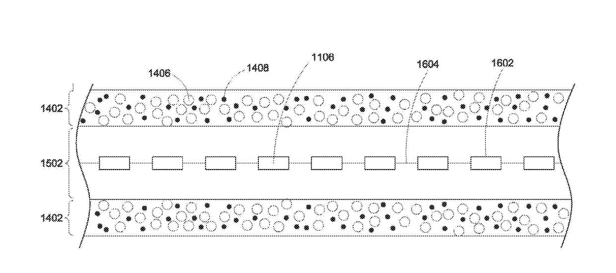
[0225]According to the second embodiment of the LED filament 200, the LED filament 200 comprises a plurality of LED chips 202, 204, at least two conductive electrodes 210, 212, and a light conversion coating 220. The conductive electrodes 210, 212 are disposed corresponding to the plurality of LED chips 202, 204. The plurality of LED chips 202, 204 and the conductive electrodes 212, 214 are electrically connected therebetween. The light conversion coating 220 coats on at least two sides of the LED chips 202, 204 and the conductive electrodes 210, 212. The light conversion coating 220 exposes a portion of two of the conductive electrodes 210, 212. The light conversion coating 220 comprises an adhesive 222, a plurality of inorganic oxide nanoparticles ...

first embodiment

[0235]Please refer to FIGS. 41A to 41E which illustrate a manufacturing method of an LED filament according to a The manufacturing method of the LED filament 200 comprises:

[0236]S20: dispose LED chips 202, 204 and at least two conductive electrodes 210, 210 on a carrier 280, referring to FIG. 41A;

[0237]S22: electrically connect the LED chips 202, 204 with the conductive electrodes 210, 212, referring to FIG. 41B; and

[0238]S24: dispose a light conversion coating 220 on the LED chips 202, 204 and the conductive electrodes 210, 212. The light conversion coating 220 coats on at least two sides of the LED chips 202, 204 and the conductive electrodes 210, 212. The light conversion coating 220 exposes a portion of at least two of the conductive electrodes 210, 212. The light conversion coating 220 comprises adhesive 222 and a plurality of phosphors 224, referring to FIG. 41C to 41E.

[0239]In S20, the plurality of LED chips 202, 204 are disposed in a rectangular array. Each column of the LE...

third embodiment

[0266]Next, please refer to FIGS. 43A to 43E which illustrate a manufacturing method of an LED filament according to a The manufacturing method for an LED filament 10a comprises:

[0267]S202: dispose conductive foil 130 on a light conversion sub-layer (base layer 120b), referring to FIG. 43A;

[0268]S204: dispose a plurality of LED chips 102, 104 and a plurality of conductive electrodes 110,112 on the conductive foil 130, referring to FIG. 43B;

[0269]S22: electrically connect the LED chips 102, 104 with the conductive electrodes 110, 112, referring to FIG. 43C; and

[0270]S24: coat a light conversion sub-layer (top layer 120a) on the surfaces of the LED chips 102, 104 and the conductive electrode 110, 112 where may be not in contact with the conductive foil 130. The light conversion coating 120 (including the base layer 120b and the top layer 120a) coats on at least two sides of the LED chips 102, 104 and the conductive electrodes 110, 112. The light conversion coating 120 exposes a porti...


PUM

PropertyMeasurementUnit
surface roughness Rzaaaaaaaaaa
transparentaaaaaaaaaa

Abstract

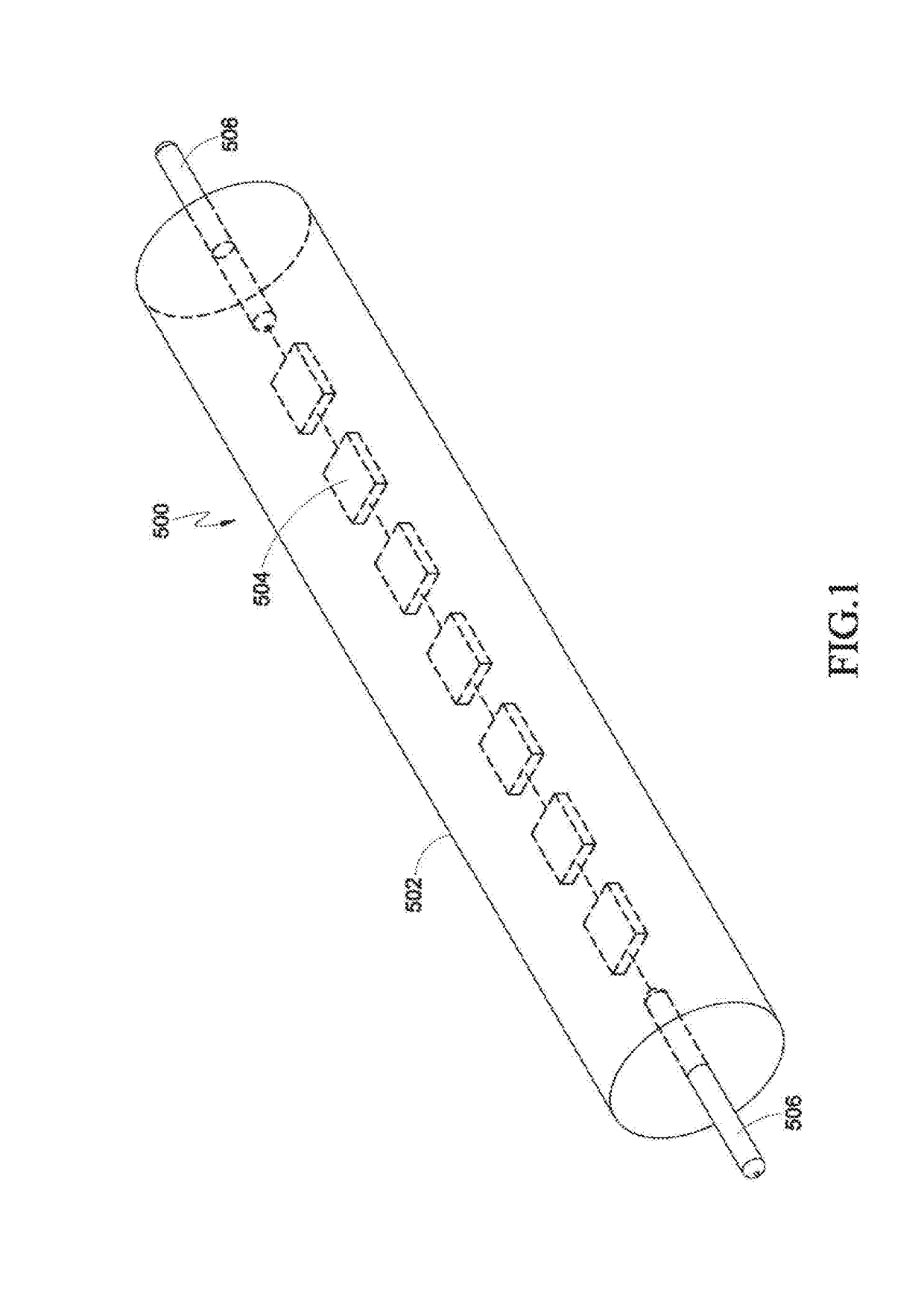
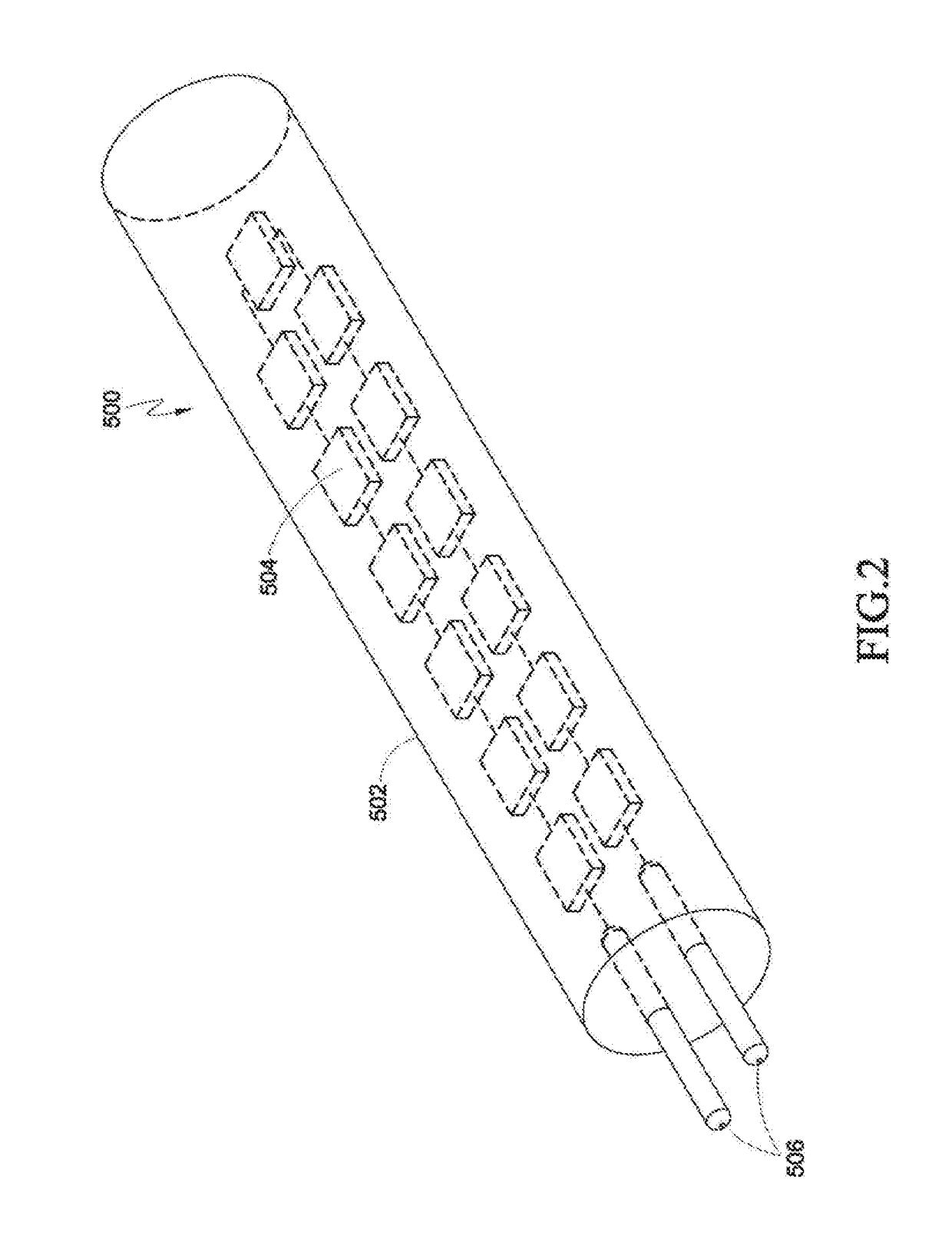
An LED filament configured to emit omnidirectional light includes a linear array of LED chips operably interconnected to emit light upon energization and a conductive electrode. The linear array of LED chips is electrically connected with the conductive electrode. A light conversion coating encloses the linear array of the LED chip and the conductive electrode. The light conversion layer includes a top layer and a base layer conformally interconnected to form a unitary enclosure. The top layer is coated on a first side of the linear array of LED chips and the conductive electrode. The base layer is coated on a second side of the linear array of LED chips and the conductive electrode.

Description

RELATED APPLICATIONS[0001]The present application claims priority to CN201510966906.3 filed Dec. 19, 2015, CN201610041667.5 filed Jan. 22, 2016, CN201610281600.9 filed Apr. 29, 2016, CN201610272153.0 filed Apr. 27, 2016, CN201610394610.3 filed Jun. 3, 2016, CN201610586388.7 filed Jul. 22, 2016, CN201610544049.2 filed Jul. 7, 2016, CN201610936171.4 filed Nov. 1, 2016 and CN201611108722.4 filed Dec. 6, 2016, each of which is incorporated herein by reference in its entirety.[0002]The present application is a continuation-in-part application of U.S. Ser. No. 15 / 366,535 filed Dec. 1, 2016, which claims priority to CN201510502630.3 filed Aug. 17, 2015, CN201510966906.3 filed Dec. 19, 2015, CN201610041667.5 filed Jan. 22, 2016, CN201610281600.9 filed Apr. 29, 2016, CN201610272153.0 filed Apr. 27, 2016, CN201610394610.3 filed Jun. 3, 2016, CN201610586388.7 filed Jul. 22, 2016, CN201610544049.2 filed Jul. 7, 2016 and CN201610936171.4 filed Nov. 1, 2016, and which is a continuation-in-part ap...

Claims


Application Information

Patent Timeline
Patent Type & Authority Applications(United States)
IPC IPC(8): F21K9/237H01L33/62F21V9/16F21V29/70F21V3/02F21K9/235F21V9/08F21V23/06H01L25/075F21K9/232
CPCF21K9/237H01L25/0753H01L33/62F21V9/16F21K9/232F21Y2115/10F21K9/235F21V9/08F21V23/06F21V29/70F21Y2103/10F21V3/02F21K9/90F21V19/003F21K9/238F21Y2103/33F21Y2103/37F21Y2107/00F21V3/061F21V3/062H01L2224/48091H01L2924/19107H01L2924/00014F21Y2107/50
Inventor JIANG, TAOLI, LIQIN
Owner ZHEJIANG SUPER LIGHTING ELECTRIC APPLIANCE
Learn More