Z-Inversion Type Display Device and Method of Manufacturing the Same

a display device and z-inversion technology, applied in semiconductor devices, electrical devices, instruments, etc., can solve the problems of affecting the quality of the display, so as to reduce or improve the non-uniformity of pixels, reduce or remove flickering or vertical line defects, and improve the effect of uniformity

Active Publication Date: 2017-05-11
LG DISPLAY CO LTD
View PDF3 Cites 0 Cited by
  • Summary
  • Abstract
  • Description
  • Claims
  • Application Information

AI Technical Summary

Benefits of technology

The present invention has the effect of maintaining uniform capacitance Cgs in a display device, even if the position of the source or drain electrodes changes. This reduces nonuniformity between pixels and improves issues such as flickering or vertical line defect. It also ensures equal capacitance in each product, eliminating the need for a secondary process to control changes.

Problems solved by technology

Among the inversion driving types, the frame inversion type, the line inversion type and the column inversion type may reduce power consumption compared to the dot inversion type, but have disadvantages in display quality degradation such as a crosstalk phenomenon or an up-down luminance difference.
However, the dot inversion type has disadvantages in that power consumption is too large compared to the line inversion type or the column inversion type.
As described above, in the case of the Z-inversion type display device, the gate electrode layer and the source / drain electrode layers may be misaligned for reasons such as a mask misalignment, and, at this time, there are problems in which the capacitances Cgs of each pixel become different.
Thus, flickering occurs or a vertical line defect occurs.

Method used


Image

  • Z-Inversion Type Display Device and Method of Manufacturing the Same
  • Z-Inversion Type Display Device and Method of Manufacturing the Same
  • Z-Inversion Type Display Device and Method of Manufacturing the Same

Examples


Embodiment Construction

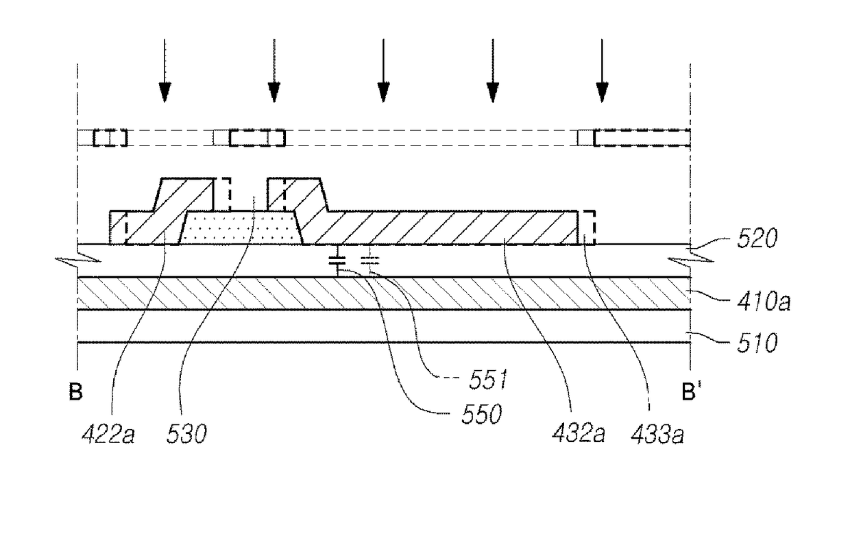
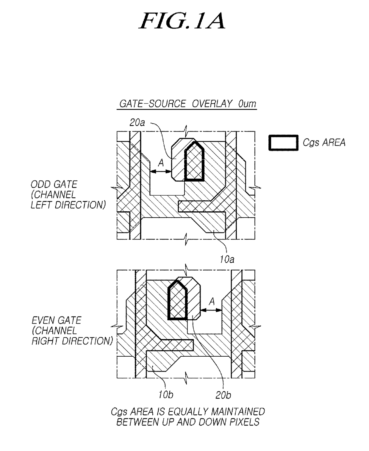
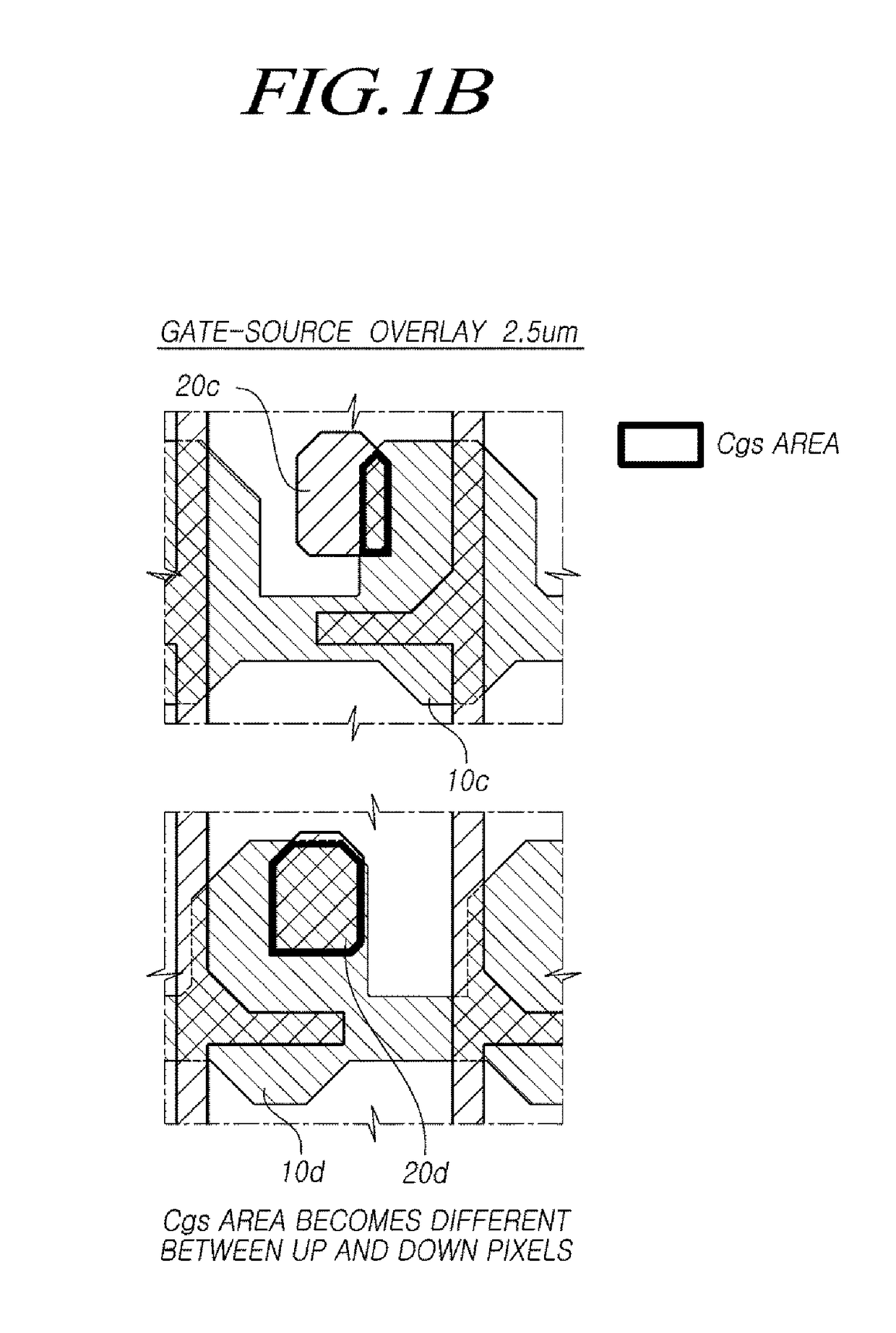
[0041]Hereinafter, embodiments of the present invention will be described with reference to the accompanying drawings. In the following description, the same components will be designated by the same reference numerals although they are shown in different drawings. Further, in the following description of the present invention, a detailed description of known functions and configurations incorporated herein will be omitted when it may make the subject matter of the present invention rather unclear.

[0042]In addition, terms, such as first, second, A, B, (a), (b) or the like may be used herein when describing components of the present invention. These terms are merely used to distinguish one structural element from other structural elements, and a property, an order, a sequence and the like of a corresponding structural element are not limited by the term. It should be noted that if it is described in the specification that one component is “connected,”“coupled” or “joined” to another ...


PUM

PropertyMeasurementUnit
viewing angleaaaaaaaaaa
areaaaaaaaaaaa
electric fieldaaaaaaaaaa

Abstract

The present invention provides a Z-inversion type display device comprising a gate line and a data line that intersect with each other to define a pixel area on a substrate, a thin film transistor that includes a gate electrode, a semiconductor layer, a source electrode and a drain electrode, and a pixel electrode that is formed in the pixel area, and is electrically connected to the drain electrode of the thin film transistor, wherein the drain electrode completely overlaps the gate line such that a drain electrode area is wholly included in a gate line area on a plan view.

Description

CROSS-REFERENCE TO RELATED APPLICATION[0001]This application is a continuation of U.S. patent application Ser. No. 14 / 699,531 filed on Apr. 29, 2015, which claims priority under 35 U.S.C. 119(a) to Republic of Korea patent application no. 10-2014-0052330 filed on Apr. 30, 2014, both of which are incorporated by reference herein in their entirety.BACKGROUND OF THE INVENTION[0002]1. Field of the Invention[0003]The present invention is a technology related to a display device and a method of manufacturing the display device. Specially, the present invention is a technology related to a display device in which pixels are formed in a Z-inversion type, and a method of manufacturing the display device.[0004]2. Description of the Prior Art[0005]With the development of the information society, various types of requirements for a display device for displaying an image are increasing and, recently, various display devices, such as a Liquid Crystal Display (LCD), a Plasma Display Panel (PDP), a...

Claims


Application Information

Patent Timeline
Patent Type & Authority Applications(United States)
IPC IPC(8): H01L27/12H01L27/32G02F1/1333G02F1/1343G02F1/1368G02F1/1362
CPCH01L27/124G02F1/1368G02F1/136286G02F1/136227G02F1/133345H01L2227/323G02F1/13439H01L27/1262H01L27/3262G02F2201/123G02F1/134309G02F1/133G02F1/1362H10K59/1213H10K59/1201
Inventor LIM, DONGGEUNSHIN, KITAEGJO, CHELHEEKANG, JIWON
Owner LG DISPLAY CO LTD
Why Eureka
Try Eureka