Unlock instant, AI-driven research and patent intelligence for your innovation.

Organic light emitting diode packaging method and packaging structure and device having the same

a light-emitting diode and organic technology, applied in the field of electronic components, can solve the problems of no light-emitting diode, no light-emitting diode, and certain limitations in use of the oled devi

Active Publication Date: 2017-06-01
BOE TECH GRP CO LTD
View PDF2 Cites 2 Cited by
  • Summary
  • Abstract
  • Description
  • Claims
  • Application Information

AI Technical Summary

Benefits of technology

The present invention provides a packaging structure for organic light emitting diodes (OLEDs) that includes a first metallic foil substrate, an OLED on top of the first substrate, a passivation layer covering the OLED, an encapsulation adhesive covering the passivation layer, and a second transparent substrate on top of the encapsulation adhesive. This structure helps to protect the OLED during production and assembly and can improve its performance and reliability.

Problems solved by technology

However, OLED devices will be damaged by corrosion under the action of water vapor and oxygen, so the OLED devices currently should be protected by a packaging structure.
Metallic foil has a strong barrier effect but has no light transmission property, and thus encounters certain limitations when in use.
Ultra-thin glass has perfect light transmission property and high barrier effect, but it is difficult to be processed.
In addition, although, in this configuration, the encapsulation adhesive is adopted to protect the OLED, water and oxygen will still permeate inside of the OLED packaging structure through the encapsulation adhesive, which leads to damage to the OLED.

Method used


Image

  • Organic light emitting diode packaging method and packaging structure and device having the same
  • Organic light emitting diode packaging method and packaging structure and device having the same
  • Organic light emitting diode packaging method and packaging structure and device having the same

Examples


example 1

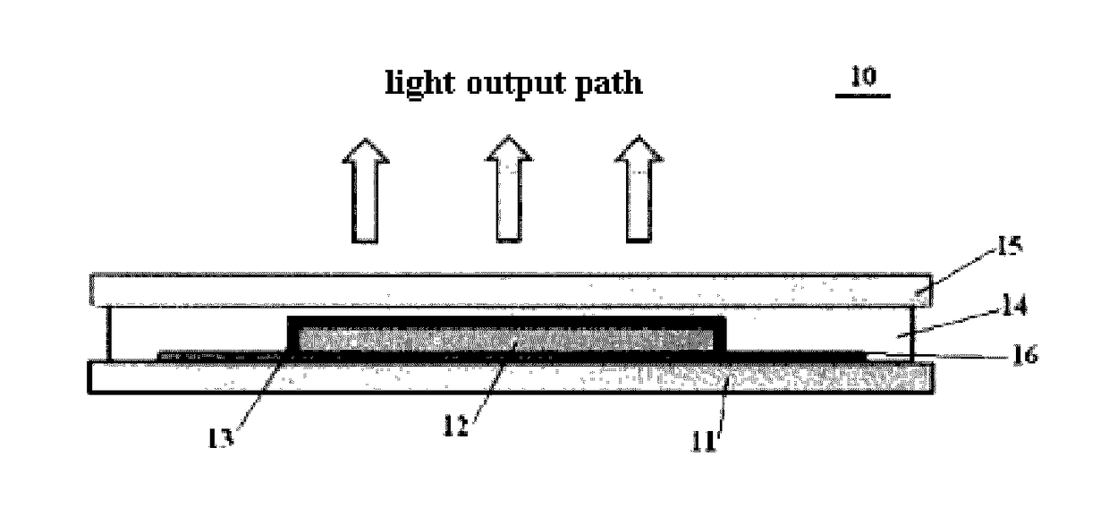
[0035]Invar alloy having a thickness of 50 μm is provided as a first substrate, and, a SiNx film having a thickness of 0.5 μm, as a planarization layer, is formed by means of CVD on the first substrate. An OLED is manufactured on the planarization layer. A SiNx film having a thickness of 1 μm, as a passivation layer, is formed by means of CVD and the passivation layer covers the OLED. Encapsulation adhesive is coated onto surface of the first substrate and covers the first substrate entirely. A plastic film, as a second substrate, is provided at least on a portion of the encapsulation adhesive covering the passivation layer. An area of a major surface of the second substrate is less than an area of a major surface of the first substrate. An edge of the first substrate is folded to enwrap the second substrate while a light emitting region is exposed, meanwhile one edge of the first substrate is kept unfolded so that a circuit portion can be extended to outside. Finally, the encapsula...

example 2

[0036]Kovar alloy having a thickness of 100 μm is provided as a first substrate, and, a plastic film having a thickness of 0.5 μm, as a planarization layer, is adhered evenly by means of being heated on the first substrate. An OLED structure is manufactured on the planarization layer. An Al2O3 film having a thickness of 0.5 μmm, as a passivation layer, is formed by means of atomic layer deposition (ALD) and the passivation layer covers the OLED. Encapsulation adhesive is coated onto surface of the first substrate and covers the first substrate entirely. A plastic film, as a second substrate, is provided at least on a portion of the encapsulation adhesive covering the passivation layer. An area of a major surface of the second substrate is less than an area of a major surface of the first substrate. An edge of the first substrate is folded to enwrap the second substrate while a light emitting region is exposed, meanwhile one edge of the first substrate is kept unfolded so that a circ...


PUM


Abstract

The present invention discloses a packaging method for an organic light emitting diode including: providing a first substrate that is made of metallic foil; providing an organic light emitting diode on the first substrate; providing, outside the organic light emitting diode, a passivation layer for covering the organic light emitting diode; coating an encapsulation adhesive onto the first substrate entirely, so that the encapsulation adhesive covers the passivation layer; providing a second transparent substrate at least on a portion of the encapsulation adhesive covering the passivation layer; and curing the encapsulation adhesive, to form a package of the organic light emitting diode. The present invention also discloses a packaging structure for an organic light emitting diode, and an organic light emitting diode device having the packaging structure.

Description

CROSS-REFERENCE TO RELATED APPLICATIONS[0001]This application is a Section 371 National Stage Application of International Application No. PCT / CN2015 / 091922, filed on 14 Oct. 2015 and entitled with “ORGANIC LIGHT EMITTING DIODE PACKAGING METHOD AND PACKAGING STRUCTURE AND DEVICE HAVING THE SAME”, which claims priority to Chinese Application No. 201510333965.7, filed on Jun. 16, 2015, which are incorporated herein by reference in their entirety.BACKGROUND[0002]1. Technical Field[0003]The present disclosure relates to the field of electronic components, and particularly to an organic light emitting diode packaging method, a packaging structure and an organic light emitting diode device having the packaging structure.[0004]2. Description of the Related Art[0005]Organic light emitting diode (OLED) is a display and lighting device that is gradually being concerned in recent years, and its characteristic of flexible displaying is especially favored by people. However, OLED devices will be...

Claims


Application Information

Patent Timeline
IPC IPC(8): H01L51/52H01L51/00H01L51/56
CPCH01L51/5253H01L51/56H01L2251/5338H01L51/5259H01L2251/301H01L51/0097H10K71/40H10K50/8426H10K50/846H10K50/844Y02E10/549H10K77/111H10K2102/3026H10K71/00H10K2102/00H10K2102/311
Inventor LUO, CHENGYUANWANG, CHUN-JAN
Owner BOE TECH GRP CO LTD