Finger pattern formation for thin film solar cells

a solar cell and finger pattern technology, applied in the field of thin film solar cell finger pattern formation, can solve the problems of high cost of electricity generated by silicon-based solar cells, large shadow loss of solar cells, and limited screen printing technique in terms of narrow finger production,

Inactive Publication Date: 2008-07-24
SOLOPOWER
View PDF21 Cites 43 Cited by
  • Summary
  • Abstract
  • Description
  • Claims
  • Application Information

AI Technical Summary

Problems solved by technology

However, the cost of electricity generated using silicon-based solar cells is higher than the cost of electricity generated by the more traditional methods.
The screen-printing technique has limitations in terms of its ability to produce narrow fingers.
Such large finger widths dramatically increase the shadowing loss in solar cells.
Such high bulk resistivity causes high resistive loses along the fingers and the busbar during operation of the solar cell.

Method used


Image

  • Finger pattern formation for thin film solar cells
  • Finger pattern formation for thin film solar cells
  • Finger pattern formation for thin film solar cells

Examples


Embodiment Construction

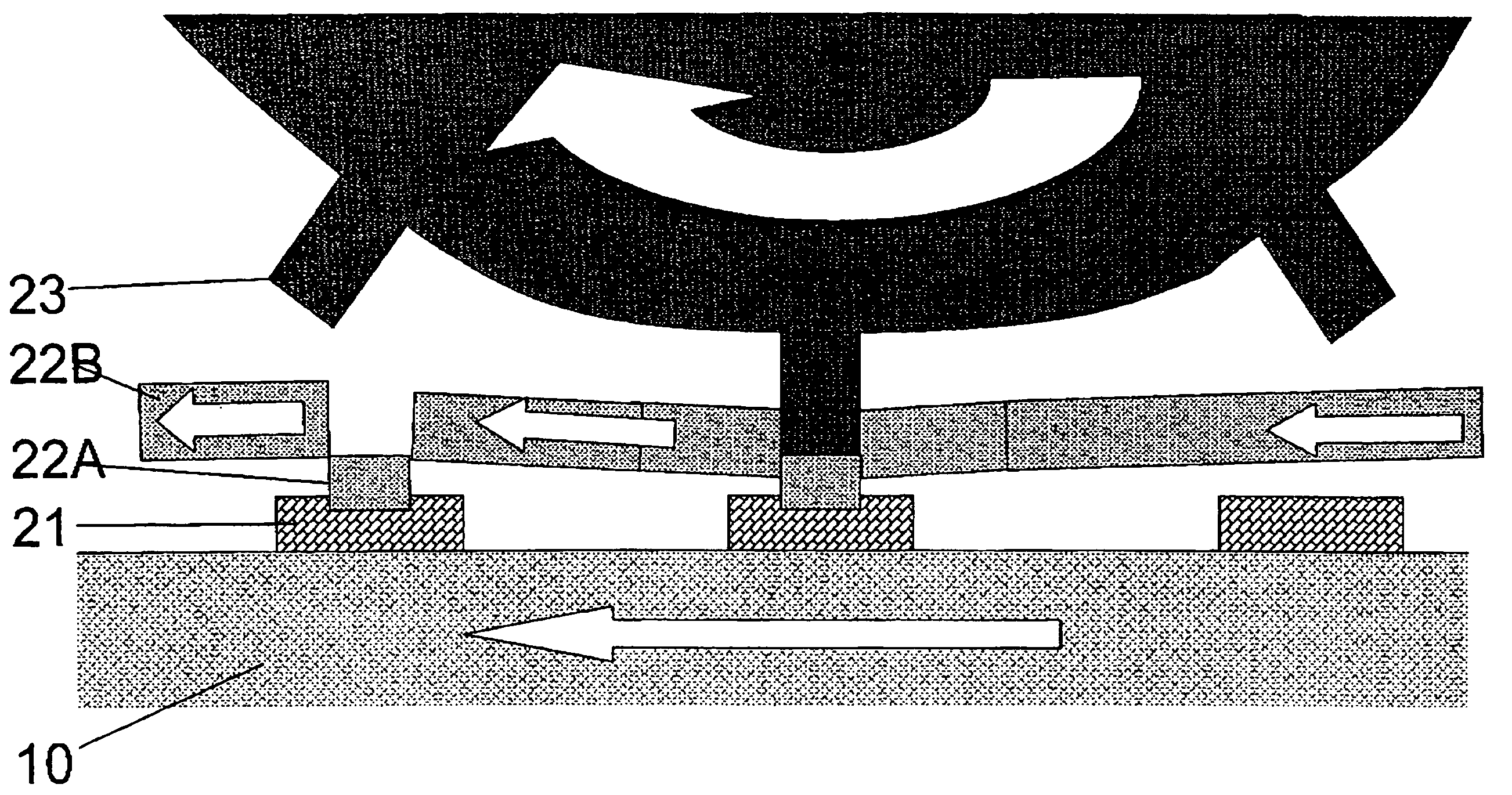
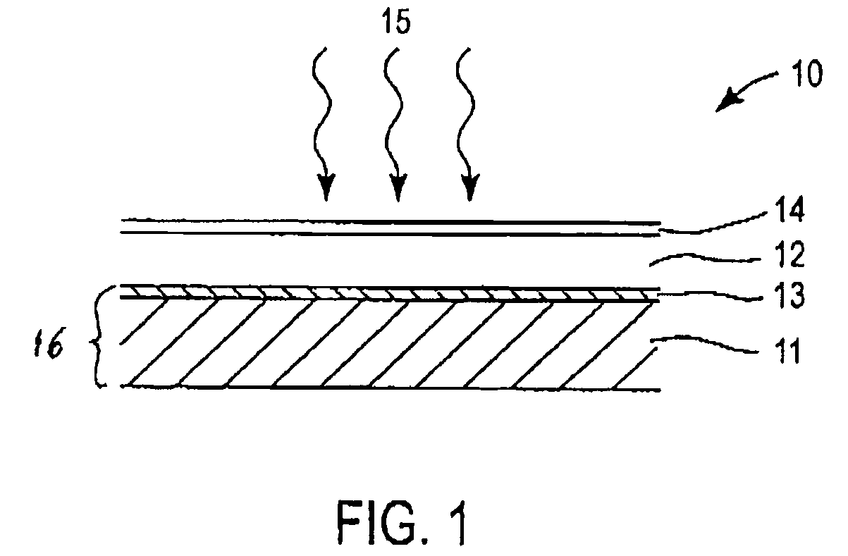
[0020]In one embodiment, the present invention forms a highly conductive metallic foil finger pattern on a solar cell structure without causing excessive shadow loss. This is achieved by transferring a highly conductive metal foil on the surface of the solar cell in the form of a finger pattern and employing a transparent conductive layer which has adhesive characteristics to attach the finger pattern on the solar cell surface. The transparent conductive layer is substantially transparent in a wavelength range of 0.45-1.2 micrometers, having an optical transmission of more than about 70%. The method will now be discussed by describing a method of forming a finger pattern or grid pattern on the device 10 which is shown in detail in FIG. 1.

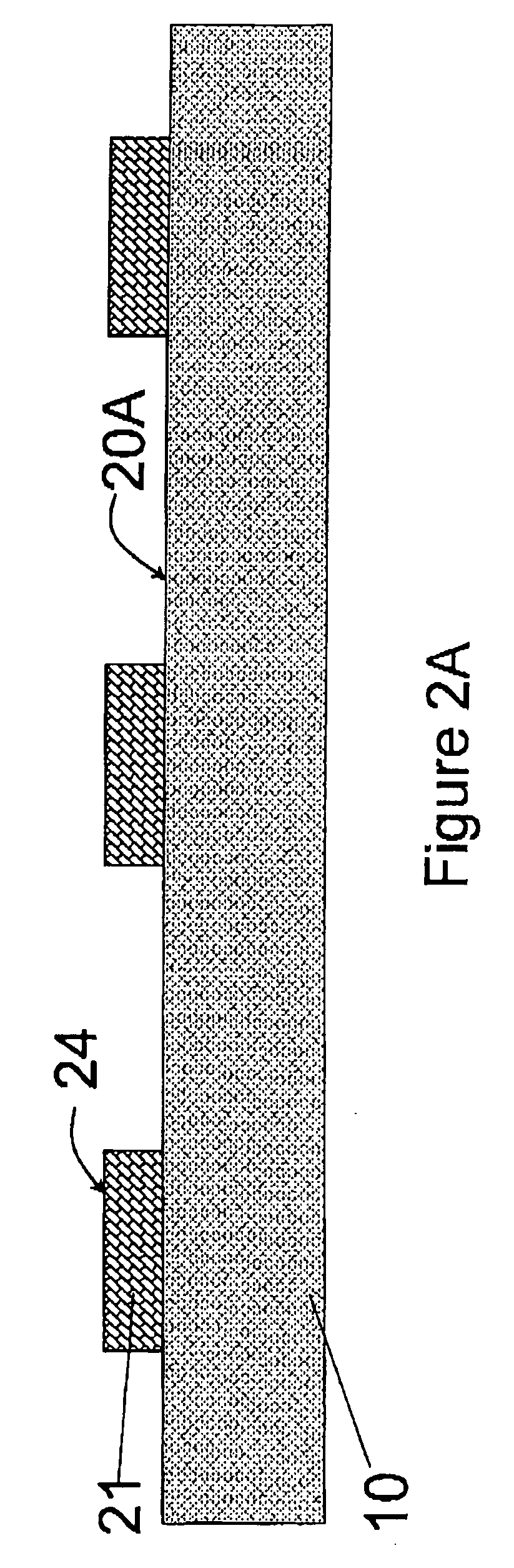
[0021]Referring to FIG. 2A, the device 10 (details of the device are shown in FIG. 1) on which the finger pattern will be formed may comprise a transparent material at its top surface 20A. As described before in reference to FIG. 1, the top surface ...


PUM

PropertyMeasurementUnit
temperatureaaaaaaaaaa
thicknessaaaaaaaaaa
widthaaaaaaaaaa

Abstract

A method of forming metallic connector patterns for solar cells, whereby an embosser having raised features shaped in the form of a metallic connector pattern is used to attach a portion of a metallic foil to a transparent conductive layer formed on a top transparent surface of a solar cell structure. The raised surfaces of the embosser press the metallic foil portion against the transparent conductive layer. Heat and pressure directed to the metallic foil portion attach the metallic foil portion to the underlying transparent conductive layer, and then the rest of the metallic foil, which is not attached to the transparent conductive layer, is removed.

Description

BACKGROUND[0001]The present application claims priority from U.S. Provisional Appln. No. 60 / 886,078 filed Jan. 22, 2007, the contents of which are incorporated herein by reference in their entirety.FIELD[0002]The present invention relates to a method and system for manufacturing thin film solar cells.DESCRIPTION OF THE RELATED ART[0003]Solar cells are photovoltaic devices that convert sunlight directly into electrical power. The most common solar cell material is silicon, which is in the form of single or polycrystalline wafers. However, the cost of electricity generated using silicon-based solar cells is higher than the cost of electricity generated by the more traditional methods. Therefore, since early 1970's there has been an effort to reduce cost of solar cells for terrestrial use. One way of reducing the cost of solar cells is to develop low-cost thin film growth techniques that can deposit solar-cell-quality absorber materials on large area substrates and to fabricate these d...

Claims


Application Information

Patent Timeline
Patent Type & Authority Applications(United States)
IPC IPC(8): B32B38/06
CPCB32B38/06B32B38/10B32B2457/12H01L31/18H05K3/041Y10T156/1041H05K2201/0326H05K2203/0108H05K2203/0143Y10T156/107Y10T156/1054H05K3/244B30B3/005
Inventor NARASIMHAN, MUKUNDANJOHNSON, TODDBASOL, BULENT M.
Owner SOLOPOWER
Why Eureka
Try Eureka