Method Of Forming Metallic Bump And Seal For Semiconductor Device

a technology of metallic bumps and seals, which is applied in the direction of semiconductor devices, semiconductor/solid-state device details, electrical devices, etc., can solve the problems of major failure of flip-chip packaging, only sitting on bumps on bumps with risky height/width ratio, and enhancing so as to enhance the mechanical robustness of bumps, enhance bonding, and increase the yield of bumping processes

Inactive Publication Date: 2009-04-16
YU WAN LING
View PDF44 Cites 43 Cited by
  • Summary
  • Abstract
  • Description
  • Claims
  • Application Information

AI Technical Summary

Benefits of technology

[0009]Accordingly, A method of forming metallic bumps on I / O pads is provided herein. A major objective of the present invention is to achieve enhanced bonding between the metallic bumps and the I / O pads and increase yield of bumping process. Another major objective is to seal up the active side of the semiconductor device in one single process. In other words, the present invention combines bumping and partial function of underfill dispensing in a single process so as to enhance the mechanical robustness of the bump. With present invention, underfill dispensing is not needed in flip-chip packaging for some semiconductor devices.

Problems solved by technology

Before underfill dispensing is completed, the bump only sits on UBM alone with a risky height / width ratio.
Bump lift is the major failure in flip-chip packaging especially when bump count is high.

Method used


Image

  • Method Of Forming Metallic Bump And Seal For Semiconductor Device
  • Method Of Forming Metallic Bump And Seal For Semiconductor Device
  • Method Of Forming Metallic Bump And Seal For Semiconductor Device

Examples


Embodiment Construction

[0013]The following descriptions are exemplary embodiments only, and are not intended to limit the scope, applicability or configuration of the invention in any way. Rather, the following description provides a convenient illustration for implementing exemplary embodiments of the invention. Various changes to the described embodiments may be made in the function and arrangement of the elements described without departing from the scope of the invention as set forth in the appended claims.

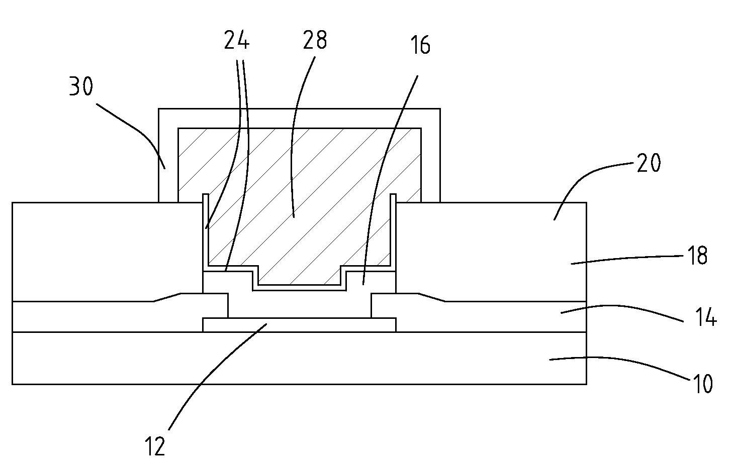
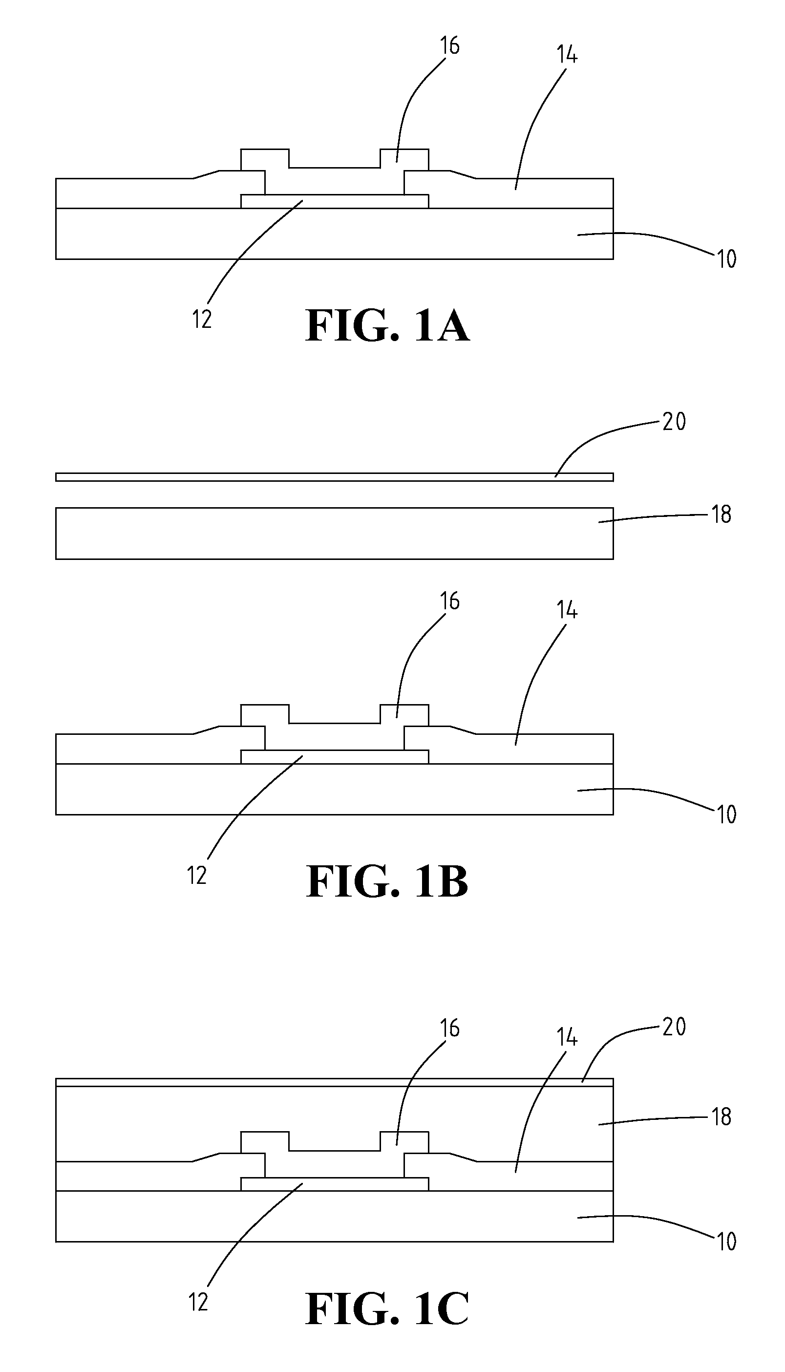
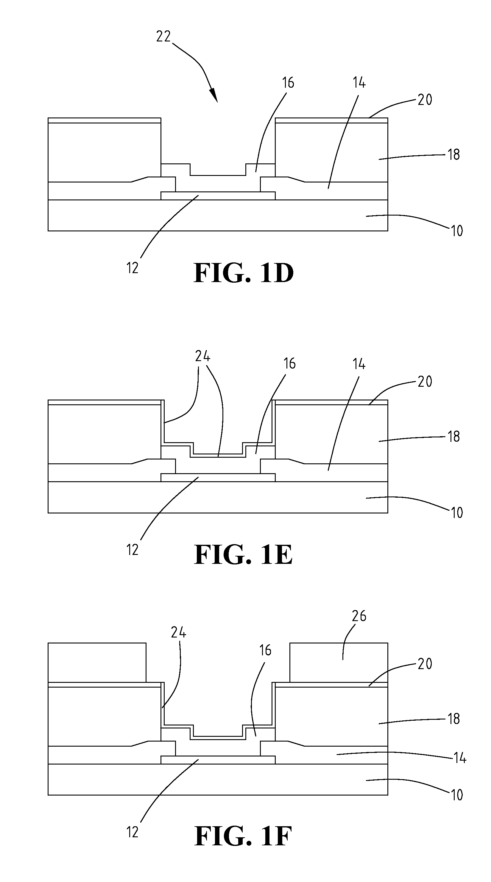
[0014]FIGS. 1A to 1H show the various steps of a method of forming a metallic bump on an I / O pad according to an embodiment of the present invention. As shown in FIG. 1A, an I / O pad 12 is located on a side of a semiconductor device 10 which can be an integrated circuit (IC), a transistor, a diode, or a thyristor. For ease of reference, this side is referred to as the active side of the semiconductor device 10. Also on the active side of the semiconductor device 10 is an optional passivation layer 14...


PUM

PropertyMeasurementUnit
metallicaaaaaaaaaa
electricalaaaaaaaaaa
adhesionaaaaaaaaaa

Abstract

The method mainly contains the following steps. First, an UBM is formed on a top side of a semiconductor's I / O pad. An isolative layer and a metallic foil are sequentially arranged in this order on the UBM. Then, a via is formed to expose the top surface of the UBM. Subsequently, a thin metallic layer is formed in the via and a resist is formed on the metallic foil. Then, by using the metallic foil and the thin metallic layer as an electrode to conduct electrical current, a metallic bump is formed using electroplating in the via on the top side of the UBM. Finally, the resist and the metallic foil are removed and the formation of the metallic bump is completed. Optionally coating on bump may be needed for certain chosen bump materials.

Description

CROSS-REFERENCES TO RELATED APPLICATIONS[0001]This is a continuation-in-part of U.S. application Ser. No. 11 / 871,974, filed Oct. 13, 2007.BACKGROUND OF THE INVENTION[0002]1. Field of the Invention[0003]The present invention generally relates to flip-chip packaging, and more particularly to a method of forming metallic bumps on the I / O pads and sealing up the active side of a semiconductor device.[0004]2. The Prior Arts[0005]Flip-chip packaging utilizes bumps to establish electrical contact between a chip's I / O pads and the substrate or lead frame of the package. Structurally, a bump actually contains the bump itself and a so-called under bump metallurgy (UBM) located between the bump and an I / O pad.[0006]An UBM generally contains an adhesion layer, a barrier layer and a wetting layer, arranged in this order on the I / O pad. The bumps themselves, based on the material used, are classified as solder bumps, gold bumps, copper pillar bumps and bumps with mixed metals.[0007]To form bumps ...

Claims


Application Information

Patent Timeline
Patent Type & Authority Applications(United States)
IPC IPC(8): H01L21/44
CPCH01L24/03H01L24/05H01L2924/0002H01L2924/1301H01L2224/11474H01L2924/00014H01L2224/05571H01L2224/05027H01L2924/01033H01L2924/01024H01L2924/14H01L2924/014H01L2924/01082H01L24/11H01L24/12H01L2224/03912H01L2224/0401H01L2224/05558H01L2224/05562H01L2224/05599H01L2224/1147H01L2224/13022H01L2224/13099H01L2224/131H01L2224/13111H01L2224/13139H01L2224/13144H01L2224/13147H01L2224/13155H01L2224/13164H01L2224/16H01L2924/01013H01L2924/01028H01L2924/01029H01L2924/01046H01L2924/01047H01L2924/0105H01L2924/01078H01L2924/01079H01L2924/00H01L2224/05552
Inventor YU, WAN-LING
Owner YU WAN LING
Why Eureka
Try Eureka