Method for producing semiconductor device and semiconductor device

a technology of semiconductor devices and semiconductor components, which is applied in the direction of semiconductor devices, semiconductor/solid-state device details, electrical devices, etc., can solve the problems of deterioration of insulating properties, reduction of resin thickness in these portions, etc., and achieve excellent insulating properties and enhanced heat dissipation properties

Active Publication Date: 2005-04-21
MITSUBISHI ELECTRIC CORP
View PDF1 Cites 37 Cited by
  • Summary
  • Abstract
  • Description
  • Claims
  • Application Information

AI Technical Summary

Benefits of technology

[0010] Using the semiconductor device producing method according to the present invention, it is possible to provide a semiconductor device in which a resin sheet and frames are fixed in a favorable fashion and which therefore exhibits an enhanced heat dissipation property and an excellent insulating property.

Problems solved by technology

While it is necessary for improvement in heat dissipation property that the resin covering the frames seating the power chips, namely, the resin between the back surfaces of the frames seating the power chips and the back surface of the semiconductor device is thin in such a semiconductor device, there is a problem that reduction in thickness of the resin disposed in these portions deteriorates an insulating property.

Method used


Image

  • Method for producing semiconductor device and semiconductor device
  • Method for producing semiconductor device and semiconductor device
  • Method for producing semiconductor device and semiconductor device

Examples


embodiment 1

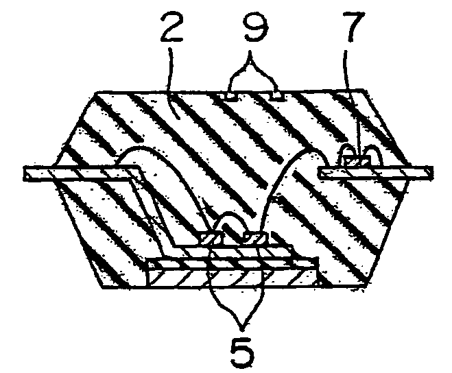
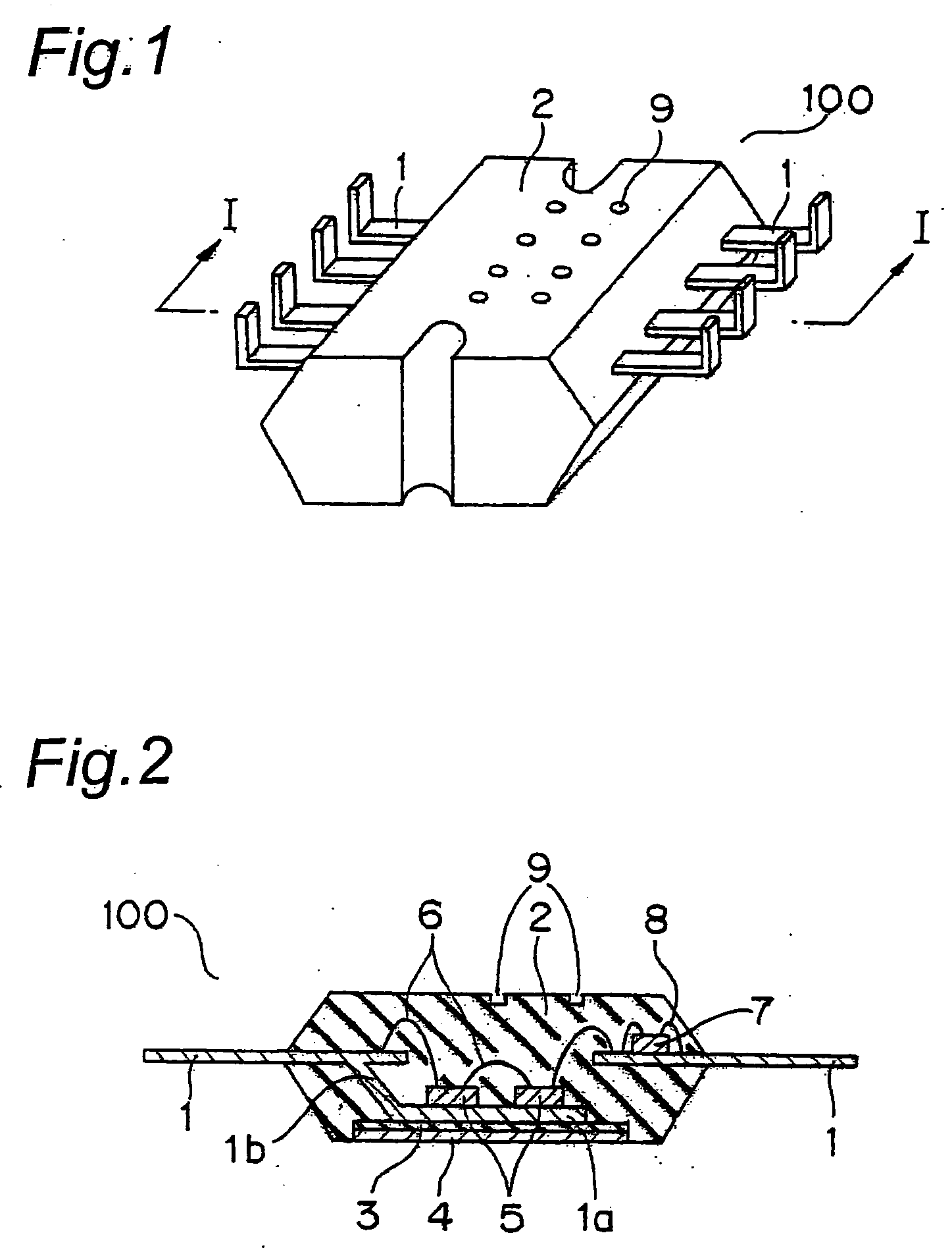
[0019]FIG. 1 is a perspective view of a semiconductor device according to this embodiment of the present invention generally denoted at 100. FIG. 2 is a cross sectional view of the semiconductor device along lines I-I in FIG. 1.

[0020] As shown in FIG. 1, the semiconductor device 100 has a resin-molded package structure and includes a mold resin 2 on the both sides of which a plurality of metal frames 1 are disposed. The mold resin 2 is preferably of an epoxy resin.

[0021] As shown in FIG. 2, the semiconductor device 100 includes the plurality of frames 1. One frame 1 seats an IC chip 7 such as a logic chip. The other frame 1 includes a die pad portion 1a and a step portion 1b, and the die pad portion 1a seats power chips 5 such as an IGBT and an FW Diode. The power chips 5, the IC chip 7 and the frames 1 are connected with each other by bonding wires 6 and 8 of gold, aluminum and the like, allowing the IC chip 7 control operations of the power chips 5. One or more power chips 5, IC...

embodiment 2

[0049]FIG. 6 is a cross sectional view of a semiconductor device according to this embodiment of the present invention generally denoted at 200, taken along the same direction as the direction I-I in FIG. 1. In FIG. 6, the same reference symbols as those in FIGS. 1 and 2 denote the same or corresponding portions.

[0050] In the semiconductor device 200, projections 29 are formed instead of the dents 9, at the same positions as those of the dents 9 of the semiconductor device 100. The projections 29 are formed as the cap pins 23 are pulled out from the upper metal mold 21 until the tips of the cap pins 23 are positioned slightly above the top surface of the mold resin 2 and the cap pins 23 are held as such at the step 6 of the producing method of the semiconductor device 100 described above with the sealing resin 12 hardened to a certain extent.

[0051] Since the semiconductor device 200 includes such projections 29, the strength of the mold resin 2, especially the bending strength, im...

embodiment 3

[0052]FIG. 7 is a cross sectional view of a semiconductor device according to this embodiment of the present invention generally denoted at 300, taken along the same direction as the direction I-I in FIG. 1. In FIG. 7, the same reference symbols as those in FIGS. 1 and 2 denote the same or corresponding portions.

[0053] The semiconductor device 300 has a structure that the dents 9 of the semiconductor device 100 are buried with a resin 30. The semiconductor device 300 is otherwise the same in structure as the semiconductor device 100. Burying with the resin 3 is accomplished using a potting method for instance.

[0054] As compared with a structure that the dents 9 are not buried, the strength and especially the bending strength improves in the semiconductor device 300.


PUM


Abstract

The method of producing a semiconductor device in which chips are resin-molded, including steps of: preparing frames having front and back surfaces and die pads; preparing an insulation resin sheet having a first and a second surfaces; preparing a resin-sealing metal mold having cap pins; mounting the resin sheet inside the resin-sealing metal mold in such a manner that the second surface of the resin sheet contacts an inner bottom surface of the resin-sealing metal mold; mounting power chips on the surfaces of the die pads; positioning the frames on the first surface of the resin sheet in such a manner that the back surfaces of the die pads contact the first surface of the resin sheet; pressing the die pads toward the resin sheet using the cap pins and fixing the die pads; injecting a sealing resin in the resin-sealing metal mold and hardening the sealing resin; and removing the semiconductor device in which the power chips are molded with the sealing resin out from the resin-sealing metal mold. The resin sheet may include a metal foil which is disposed to the second surface.

Description

CROSS-REFERENCE TO RELATED APPLICATION [0001] The disclosure of Japanese Patent Application No. 2003-358815 filed on Oct. 20, 2003 including specification, drawings and claims is incorporated herein by reference in its entirety BACKGROUND OF THE INVENTION [0002] 1. Field of the Invention [0003] This invention relates to a method of producing a semiconductor device, and more particularly, a method of producing a power semiconductor device including a power chip. [0004] 2. Description of the Related Art [0005] In a power semiconductor device having a conventional structure, a power chip, an IC chip and the like are each die-bonded on a frame and these chips are sealed with a resin. Since a power chip has large heat dissipation, a cooling fin is attached to the back surface of the semiconductor device for instance to thereby enhance a heat dissipation efficiency. The frames seating the power chips are coated with a resin and insulated from the cooling fin which is attached to the back ...

Claims


Application Information

Patent Timeline
Patent Type & Authority Applications(United States)
IPC IPC(8): H01L25/18H01L21/56H01L23/28H01L23/29H01L23/433H01L23/495H01L25/04
CPCH01L21/565H01L2924/1815H01L23/49575H01L24/45H01L24/49H01L2224/45124H01L2224/45144H01L2224/48091H01L2224/48137H01L2224/48247H01L2224/4903H01L2224/49051H01L2924/01004H01L2924/01005H01L2924/01006H01L2924/01013H01L2924/01014H01L2924/01027H01L2924/01029H01L2924/01033H01L2924/01047H01L2924/01079H01L2924/01082H01L2924/13055H01L2924/14H01L23/4334H01L2924/014H01L24/48H01L2924/00014H01L2924/00H01L2924/181H01L2924/00012H01L23/28
Inventor HAYASHI, KENICHIKAWAFUJI, HISASHITAKESHITA, TATSUYUKIFUNAKOSHI, NOBUHITOOZAKI, HIROYUKI
Owner MITSUBISHI ELECTRIC CORP
Why Eureka
Try Eureka